

Application Gallery
Vertical Photodetector
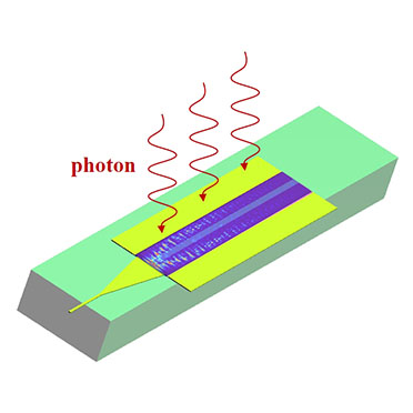
A vertical photodetector is a core optoelectronic device that converts optical signals into electrical signals. Its typical structure consists of a germanium ( Ge ) absorption layer integrated above a silicon waveguide. Light is vertically coupled from the silicon waveguide into the Ge layer through a tapered coupling structure and absorbed, generating electron-hole pairs, which are separated under the built-in electric field to form a photocurrent. Based on reference [1], this example simulates a vertical Ge-Si photodetector, using the eigenmode expansion (EME) solver to optimize the device dimensions and the finite-difference time-domain (FDTD) solver to calculate parameters such as the photo-generated carrier generation rate.
Photonic Crystal Slab
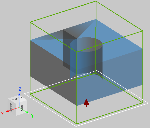
A photonic crystal is an artificial microstructure whose dielectric constant is periodically distributed in space. Its period is comparable to the wavelength of light, allowing effective control of light propagation. In this case, the rigorous coupled-wave analysis (RCWA) method is used to simulate the reflection and transmission characteristics of a square-lattice two-dimensional photonic crystal slab with circular holes, analyze their variation with frequency, incident angle, and polarization state, and determine the influence of the maximum number of k-vectors on computational accuracy through a convergence test.
PN Junction Diode
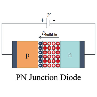
A PN junction diode is a two-terminal device formed by the contact between a p-type semiconductor and an n-type semiconductor. It features unidirectional conductivity, a simple structure, and ease of integration. By applying an external bias, the width of the depletion region and the barrier height can be modulated, enabling functions such as current rectification and switching. Compared with traditional vacuum tubes, PN junction diodes offer advantages such as small size, low power consumption, and fast response. This example uses the finite-difference charge transport (FDCharge) solver to simulate an ideal silicon PN junction diode, obtaining key parameters including the band structure, built-in voltage, depletion region width, current-voltage characteristics, and junction capacitance, and verifying the consistency between the simulation results and the analytical model.
Vortex Beam Metasurface
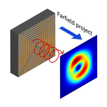
A metasurface is a structure composed of periodically arranged subwavelength units. It offers advantages such as being lightweight and thin, low-loss, and easy to integrate, and can manipulate electromagnetic waves through the phase discontinuities it generates, enabling functions such as focusing and shaping of light beams. Compared with traditional optical devices, metasurfaces can flexibly adjust the amplitude and phase of light beams. Based on reference [1], this example uses the finite-difference time-domain (FDTD) method to simulate a metasurface that can generate a vortex beam, and uses far-field projection to obtain the intensity distribution of the beam at a distance of 50 wavelengths from the metasurface.
Edge Coupler
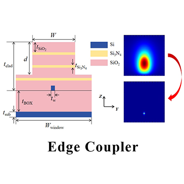
The edge coupler is a key device that enables efficient coupling between optical fibers and on-chip waveguides at the chip facet. It is widely used in low-loss fiber-to-chip coupling interfaces, optical input/output (I/O) at chip facets, and optical probe coupling in wafer-level testing. This example, based on reference [1], uses the finite-difference eigenmode (FDE) solver and the eigenmode expansion (EME) solver to model and simulate an edge coupler operating at 1550 nm that achieves efficient coupling between a standard SMF-28 single-mode fiber and a chip.
Phase-Shifted Bragg Grating
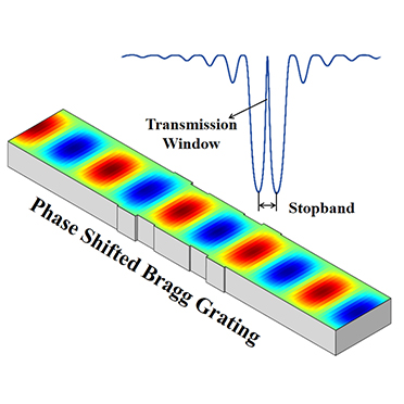
A phase-shifted Bragg grating (PSBG) is an optical device formed by introducing one or more phase jump points into the periodic structure of a conventional Bragg grating. It can open one or more extremely narrow transmission windows within the stopband of the grating's transmission spectrum, and can be used as a narrowband bandpass filter and wavelength selector in optical fiber communications, lasers, sensing, and other fields. This example uses the EME solver to simulate a phase-shifted Bragg grating, calculate its transmission spectrum, and analyze the influence of the number of periods on the grating's filtering characteristics.
Spot Size Converter
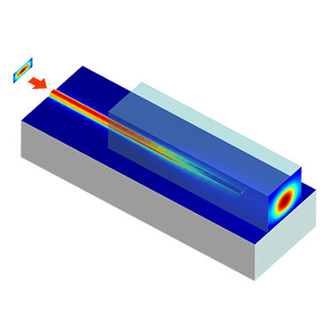
Waveguides are fundamental components in integrated photonic chips, used to transmit optical signals within the chip. However, the mode field sizes of waveguides and optical fibers typically differ significantly, leading to high coupling losses when directly connected. Therefore, a Spot Size Converter (SSC) is often employed as an intermediate transition structure. Based on reference [1], this example simulates a spot size converter using a tapered waveguide with a polymer overlay, utilizing the EME solver.
Polarization Rotator
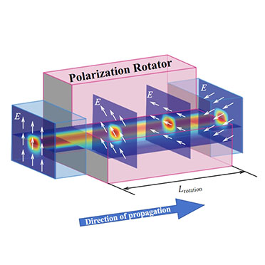
A polarization rotator (PR) is a special waveguide structure that enables mutual conversion between polarization states by accumulating the phase difference between the TE and TM modes. It is widely used in coherent optical communications, polarization‑division multiplexed photonic integrated circuits, and quantum information processing. This example introduces the simulation method for a polarization rotator and demonstrates two approaches for calculating the rotation length using the FDE and EME solvers.
Reflection and Transmission Calculations Using a Plane Wave
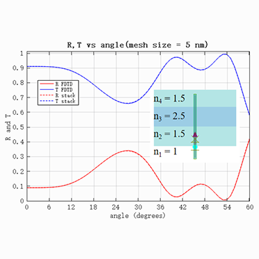
For laterally uniform multilayer structures with refractive index variations only in the thickness direction, the stack script provides an efficient analytical calculation method. Based on the transfer matrix method (TMM), the stack script associates each layer with a transfer matrix, multiplies the matrices sequentially to obtain the overall transfer matrix, and then solves for the reflectance, transmittance, and field distribution of the structure. Using a four-layer dielectric structure as an example, this page compares the transmittance and reflectance at different incident angles obtained from the stackrt script and the FDTD method. In addition, the stackrt script is used to analyze the effect of a 5 nm thickness variation in the middle layers on the reflectance.

Polarization Converter Using A Tapered Waveguide
The tapered-waveguide-type polarization converter achieves efficient polarization conversion by enabling smooth energy coupling between different polarization modes through a gradually varying waveguide cross-section along the propagation direction. This structure offers advantages such as broad bandwidth, low loss, and high tolerance to fabrication errors, making it widely used in optical communications, polarization multiplexing, and polarization control in silicon photonic chips. In this example, the FDE solver is first used to sweep the waveguide width and analyze the variation of the effective refractive index of the TM1 and TE0 modes, identifying the region where the two modes intersect to guide the design range of the tapered waveguide. Subsequently, the FDTD and EME solvers are employed to perform three-dimensional simulations of the entire structure to calculate the light propagation and polarization conversion efficiency within the tapered waveguide. By comparing the speed and accuracy of the two solvers, the unique advantages of EME in planar waveguide design are validated.