

Electrical Simulation of Planar Solar Cell
Preface
With the growing global demand for clean energy, solar energy, owing to its inexhaustible supply and zero carbon emissions, has become one of the most promising renewable energy sources. Solar cells are the core devices for photoelectric conversion. The basic principle is that when sunlight illuminates a semiconductor material with photovoltaic effect, the semiconductor absorbs photons and generates photogenerated carriers, which then form a photocurrent under the built‑in electric field or electrode action.
As solar cell designs become more complex, accurate numerical simulation has become a critical tool for predicting and optimizing device performance. The FDTD solver can compute the photogenerated carrier generation rate in the solar cell, and this rate can be imported into the FDCharge solver for electrical simulation to determine key metrics of the solar cell. This case study demonstrates the calculation of current–voltage characteristics and other metrics by importing optical simulation results (for details, please refer to Planar Silicon Solar Cell).
Simulation settings
Device introduction
In this case study, the photogenerated carrier generation rate is imported into Solar, and the simulation yields metrics such as short‑circuit current density and photovoltaic conversion efficiency.
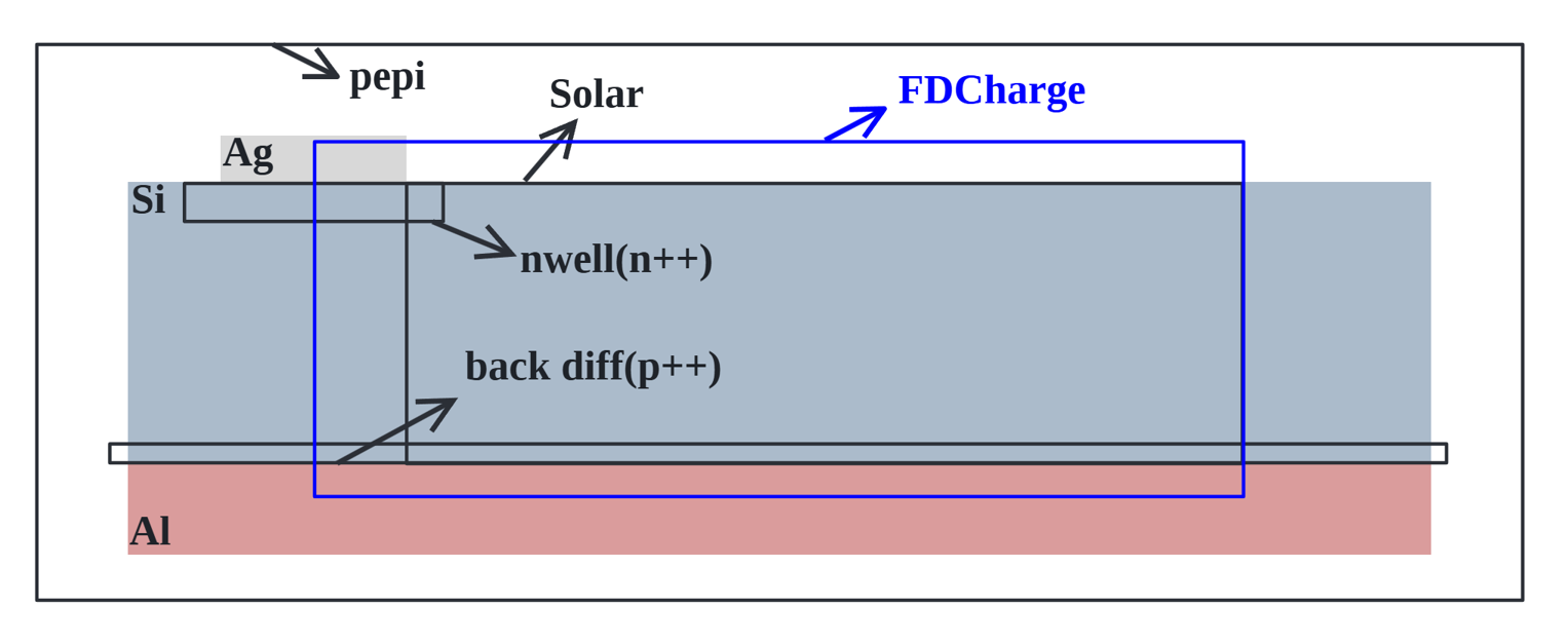
The material settings are shown in the figure above. The FDCharge solver has a dedicated active material library (Electrical Material). The basic structure of the solar cell consists of silicon (Si), silver (Ag), and aluminium (Al). Si is the semiconductor substrate of the device and is the core medium for all carrier generation, transport, and recombination calculations. Different doping profiles are added to Si to establish the built‑in electric field and to control carrier transport behavior, as detailed below: a uniform P‑type doping is applied throughout the Si region with a concentration of ; an N‑type diffused doping is placed under the Ag contact with a concentration of ; and a P‑type diffused doping is placed above the Al contact with a concentration of .
Simulation Results
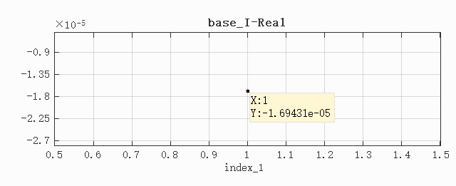
The Si material model used in the simulation incorporates some non‑ideal characteristics, such as bulk recombination effects. The Si_bulk material model is selected, which includes Shockley‑Read‑Hall (SRH) recombination, radiative recombination, and Auger recombination. After running the simulation, the short‑circuit current at zero base voltage is found to be . To obtain the more commonly used short‑circuit current density, the result must be normalized to the device area, which is given by the simulation's norm length multiplied by the x‑span. From this, the short‑circuit current density obtained with the Si_bulk model is calculated to be , i.e., .
The photovoltaic conversion efficiency is commonly used to evaluate solar cell performance, and its expression is:
where is the fill factor, is the open‑circuit voltage, is the short‑circuit current density, and is the incident power under the AM1.5G solar spectrum model [1], with a value of .
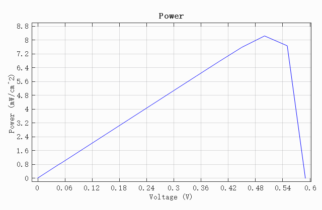
The fill factor is related to the maximum power point, i.e., the maximum of the product of current and voltage:
Therefore, the photovoltaic conversion efficiency can also be written as:
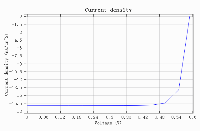
Running the script accompanying this case study yields the current–voltage characteristics of the solar cell. In addition, the script generates the power curve for calculating the conversion efficiency and displays the open‑circuit voltage, short‑circuit current, maximum power, fill factor, and conversion efficiency in the Script Console. When Si includes the aforementioned three bulk recombination mechanisms, the photovoltaic conversion efficiency is .
| () | () | () | () | |
|---|---|---|---|---|
| 0.602230 | 16.6902 | 8.19662 | 0.815477 | 8.19662 |
References
[1] Standard Tables for Reference Solar Spectral Irradiances: Direct Normal and Hemispherical on 37° Tilted Surface, ASTM G 173-2003, 2003.