

Polarization Converter Using A Tapered Waveguide
Preface
Polarization converters are optical devices capable of efficiently transforming the polarization state of incident light from one form (e.g., TM mode) to another (e.g., TE mode). They play an important role in integrated photonics and polarization control applications. Common polarization converter designs include asymmetric waveguide sidewalls, stress-induced birefringence structures, and tapered waveguides with geometrical gradients. Among them, the tapered-waveguide-type polarization converter achieves efficient polarization conversion by enabling smooth energy coupling between different polarization modes through a gradually varying waveguide cross-section along the propagation direction. This structure offers advantages such as broad bandwidth, low loss, and high tolerance to fabrication errors, making it widely used in optical communications, polarization multiplexing, and polarization control in silicon photonic chips.

In this example, the FDE solver is first used to sweep the waveguide width and analyze the variation of the effective refractive index of the and modes, identifying the region where the two modes intersect to guide the design range of the tapered waveguide. Subsequently, the FDTD and EME solvers are employed to perform three-dimensional simulations of the entire structure to calculate the light propagation and polarization conversion efficiency within the tapered waveguide. By comparing the speed and accuracy of the two solvers, the unique advantages of EME in planar waveguide design are validated.
Simulation settings
Device Construction
This example employs an SOI tapered rib waveguide structure, as shown in the figure above. The waveguide consists of a glass substrate overlaid with a -thick silicon layer, on top of which a -high rib is formed. The rib width gradually decreases along the propagation direction, and the values of and are determined from the FDE simulation. The refractive index of the materials are set to and , consistent with Ref. [1].
Source
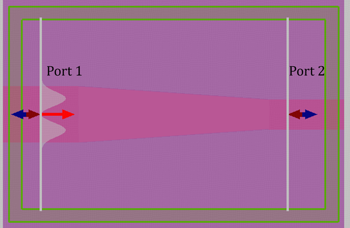
In the FDTD simulation, a Port group is used as the source. The model contains two ports, located at the positions of Port 1 and Port 2 shown in the figure below, with Port 1 serving as the input port.
Since this example focuses on the polarization conversion from the mode to the mode, the Mode Selection option in the port settings is set to User Select. The mode is selected as the input mode at Port 1, while Port 2 is set to detect the , , and modes in order to analyze the output mode composition.
Simulation results
Mode Crossing Point
Open the taper_width_sweep.mpps project and run the simulation. Save the first five eigenmodes to the Modes workspace to enable mode matching during the subsequent waveguide width sweep. Then run the taper_width_sweep.msf script. The script automatically sweeps the rib width from down to , and records the variation of the effective refractive index () of the first five modes with respect to the waveguide width. To remove the contribution of the underlying slab to and ensure that the resulting effective index variation reflects only the effect of the rib structure on the mode properties, the obtained values are subtracted by the reference value of the slab waveguide (without ribs), = 2.754047.
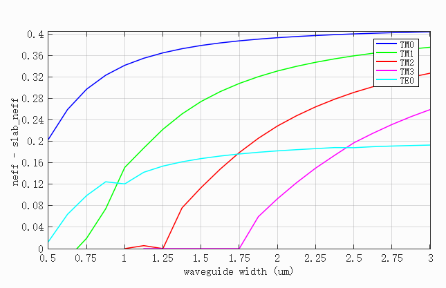
The sweep results, as shown in the figure above, indicate that the neff curves of the and modes intersect at a waveguide width of approximately . This region marks the key width range where mode coupling and polarization conversion occur.
Mode Conversion Efficiency using FDTD
Based on the FDE simulation results, the waveguide width at the input and output ends in the subsequent FDTD simulation are set to and , respectively. This width range is consistent with the design in reference [1:1], ensuring that the tapered waveguide effectively covers the mode crossing region between and .
At Port 1 (waveguide width ), the mode is selected as the input source, while at Port 2 (waveguide width ), the , , and modes are selected as the output monitors.
The attached pol_converter.mpps project includes a parameter sweep that varies the taper length ().
After the sweep, the -parameters obtained at Port 2 represent the mode conversion efficiencies: for the transition from to , for the transition from to , and for the transition from to .
Since the simulation is computationally intensive, the sweep range in the attached project is set to . To provide a more complete view of the mode conversion trend, the results shown in this example extend the sweep range to , as illustrated in the figure below.
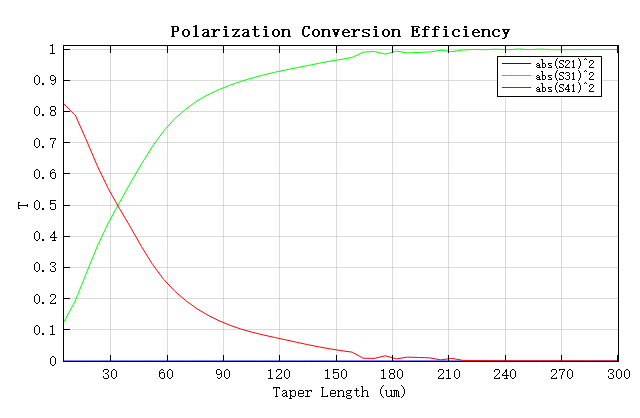
The results show that the mode transfers almost no power to the mode. As the taper length increases, the mode gradually converts into the mode. When the taper is sufficiently long, the mode can be efficiently converted into the mode with negligible loss, achieving high polarization conversion efficiency.
Mode Conversion Efficiency using EME
In the FDTD-based calculation above, a sweep over the taper length was performed. To reduce the computational burden, the sweep range in the attached project was set to with 51 points, which corresponds to 51 individual FDTD simulations—a time‑consuming process that significantly affects efficiency. Therefore, the Eigenmode Expansion (EME) solver can be utilized instead. The EME method is specifically designed for planar waveguide structures and is particularly well‑suited for large‑scale, long‑distance optical propagation simulations.
Open the attached pol_converter_EME.mpps project and run the Pol_converter_EME.msf script. After execution, the script directly plots the mode conversion efficiency for taper lengths ranging from , with the entire process taking less than 90 seconds. Compared to the FDTD solver, the EME solver not only offers significantly faster computation but also achieves high accuracy.
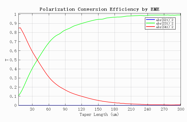
When dealing with large-scale, long-distance optical propagation simulations, the FDTD solver is constrained by the Courant stability condition, causing its simulation time to increase rapidly with the structural size. In contrast, the EME solver is based on mode‑coupling theory, which efficiently decomposes any arbitrary input field into a linear combination of eigenmodes of the waveguide cross‑section, and solves Maxwell's equations in the frequency domain with appropriate boundary conditions. This approach accurately computes mode coupling and evolution while significantly improving computational efficiency without sacrificing accuracy. Specifically designed for planar waveguide structures, this method has become the preferred tool for simulating the transmission characteristics of complex waveguide systems in the development of integrated optical devices.