

Spot Size Converter
Preface
Waveguides are fundamental components in integrated photonic chips, used to transmit optical signals within the chip. However, the mode field sizes of waveguides and optical fibers typically differ significantly, leading to high coupling losses when directly connected. Therefore, a Spot Size Converter (SSC) is often employed as an intermediate transition structure. The Eigenmode Expansion (EME) solver is based on mode‑coupling theory, which efficiently decomposes any arbitrary input field into a linear combination of eigenmodes of the waveguide cross‑section, and solves Maxwell's equations in the frequency domain with appropriate boundary conditions. This approach accurately computes mode coupling and evolution, and is particularly well‑suited for waveguide structures with slowly varying longitudinal cross‑sections but long propagation distances, enabling efficient design and length optimization of tapered waveguides. Based on reference [1], this example simulates a spot size converter using a tapered waveguide with a polymer overlay, utilizing the EME solver.
Simulation settings
Structure Description
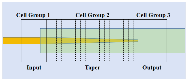
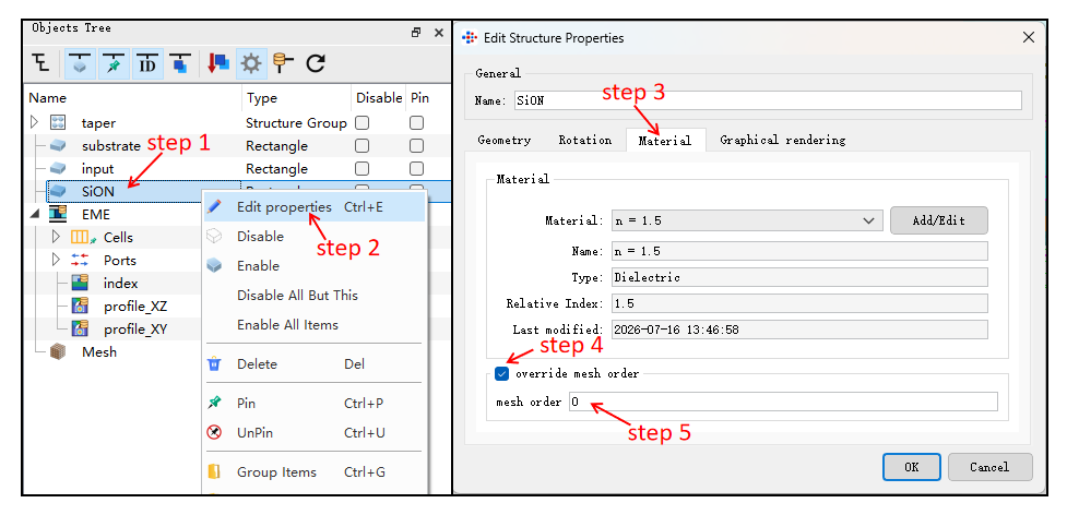
The spot size converter consists of a substrate, an input waveguide, a tapered waveguide, and a low‑index polymer waveguide overlaid on the tapered section. Since the low‑index polymer waveguide overlaps spatially with the tapered waveguide and part of the input waveguide, the mesh order needs to be set to control the material selection in the overlapping regions. A higher mesh order indicates a higher material priority. Therefore, the mesh order of the input waveguide and the tapered waveguide must be set higher than that of the low‑index polymer waveguide. For example, set the mesh order of the input and tapered waveguides to , and that of the low‑index polymer waveguide to . The specific procedure is: select the structure, right‑click to open the edit window, switch to the Material tab, check the override mesh order option (disabled by default), and set the mesh order value, as shown in the figure below.
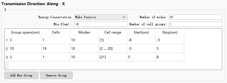
In the EME solver settings, three cell groups need to be defined, corresponding to the input waveguide, the tapered waveguide, and the output waveguide regions. For sections with constant cross‑section (e.g., input and output waveguides), only one cell is needed per cell group; for the tapered region where the cross‑section varies slowly, more cells are required to accurately resolve the structural changes, with the specific settings shown in the figure below. Since the structure does not contain any periodic sections, the periodicity settings can be ignored. For periodic structures, refer to the Fiber Bragg Grating example.
Simulation Results
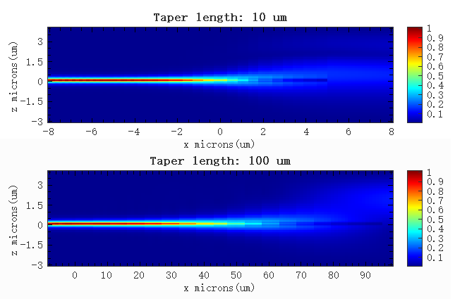
The EME method divides the waveguide into several segments, solves for the eigenmodes within each segment, and rigorously computes mode coupling and transmission through mode matching. It is particularly well‑suited for waveguide structures with constant or slowly varying cross‑sections along the propagation direction but long propagation distances, such as tapered waveguides. Open the attached spot_size_converter.mpps project and run the run; emepropagate command in the script console. After the simulation finishes, the results can be viewed in the monitors. To change the tapered waveguide length, there is no need to rebuild the geometry; simply modify the length of the second cell group in the EME Analysis Window and click the EME Propagate button or run the emepropagate command in the script console to quickly obtain results for the new length. The figure below shows the electric field distribution in the XZ plane for taper lengths of and .
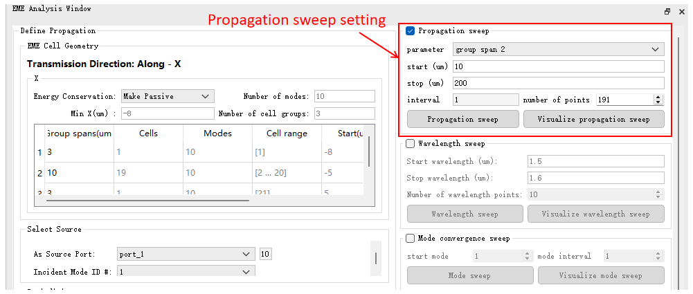
To obtain the relationship between taper length and transmission, the Propagation Sweep function of EME can be used. In the EME Analysis Window, enable Propagation sweep, select group span 2 as the parameter, set the length sweep range from to , and set the number of sweep points to , as shown in the figure below. Thanks to the efficiency of the EME mode‑matching algorithm, the entire length sweep takes only a few seconds, significantly faster than FDTD‑based methods. Click the Propagation sweep button, and the sweep results are automatically stored in the EME S‑matrix.
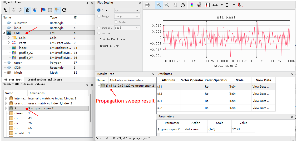
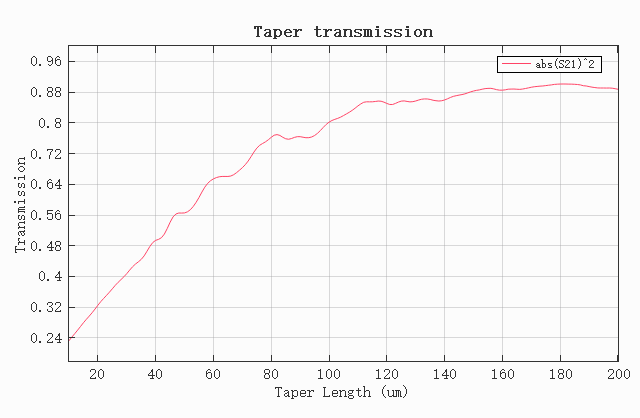
For this spot size converter, the power transmission coefficient from the fundamental mode of the silicon waveguide at Port 1 to the fundamental mode of the polymer waveguide at Port 2, i.e., , is of interest. Due to the symmetry of the device, the same result can be obtained from . Click Visualize propagation sweep to view the transmission curve, or run the attached script spot_size_converter.msf to plot it directly. The figure below shows the transmission as a function of taper length, with slight fluctuations due to the staircasing effect.
Constrained by the Courant stability condition, the simulation time of the FDTD solver increases rapidly with structural size when dealing with large‑scale, long‑distance optical propagation simulations. In contrast, the EME method is specifically designed for planar waveguide structures and is well‑suited for the design and optimization of tapered waveguides, making it an important tool for simulating the transmission characteristics of complex waveguide systems in the development of integrated optical devices.
References
[1] T. Tsuchizawa et al., "Microphotonics devices based on silicon microfabrication technology," IEEE J. Select. Topics Quantum Electron., 11(1), 232-240 (2005).
