

Edge Coupler
Preface
There are two common devices for efficient coupling between optical fibers and on-chip waveguides at the chip facet: grating couplers and edge couplers. Grating couplers can perform vertical or angled coupling at any position on the chip and do not require additional processing of the chip edge; however, because they are based on the dispersion principle, their working bandwidth may be limited. Edge couplers, on the other hand, operate independently of wavelength and can provide a larger working bandwidth, but they require additional cutting and polishing processes at the chip edge to form the coupling facet. They are currently widely used in low-loss horizontal coupling interfaces for fiber-to-chip coupling, optical input/output (I/O) at chip facets, and optical probe coupling in wafer-level testing. By building a gradual mode-field transition structure at the chip edge, an edge coupler can gradually convert and compress the larger spot mode of the fiber into the on-chip waveguide, thereby solving the severe mode-field mismatch between the two. It is a fundamental component for achieving low-loss optical interconnection between fibers and chips. The following table summarizes the main characteristics of the two types of couplers:
| Characteristic | Grating Coupler | Edge Coupler |
|---|---|---|
| Coupling direction | Vertical or angled | Horizontal |
| Coupling loss | Higher | Low |
| Working bandwidth | Narrow | Extremely wide |
| Chip edge treatment | Not required | Cutting and polishing required |
| Coupling position | Anywhere on the chip | Chip edge |
The eigenmode expansion (EME) solver can discretize the device into multiple uniform cross-section cells along the propagation direction and calculate the S-parameters between adjacent cells, rapidly obtaining the spectral response of the entire structure for any length. It is especially suitable for scanning and optimizing the length of tapered waveguides. Based on reference [1], this example uses the finite-difference eigenmode (FDE) solver and the EME solver to model and simulate an on-chip silicon-on-insulator (SOI) edge coupler operating at 1550 nm that can achieve efficient optical coupling between a standard SMF-28 single-mode fiber and a chip.
Simulation Settings
Structure Description
The SMF-28 single-mode fiber used in this example consists of a cladding and a core. The core radius is 4.1 μm and the refractive index is 1.44; the cladding radius is 20 μm and the refractive index is 1.434816. A schematic of the edge coupler structure is shown below. The edge coupler in reference [1] has three important components:
- A three-layer Si3N4 waveguide structure, used to expand the optical field into a wider waveguide mode to improve compatibility with the fiber mode;
- An inversely tapered silicon waveguide, whose width varies along the device length;
- A subwavelength grating (SWG) structure, which gradually reduces the effective refractive index of the mode from Si3N4 to SiO2.
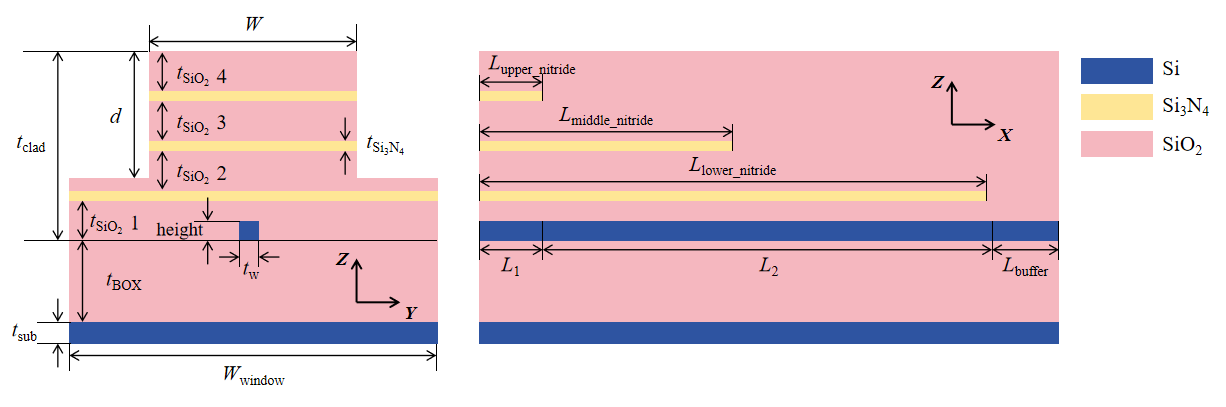
In the simulation project, the subwavelength grating structure is not actually built. Instead, an equivalent graded refractive index is used as an approximation, assuming that the effective refractive index of the Si3N4 layer can gradually change from that of Si3N4 to that of SiO2 along the device length. The simulation file uses a Structure Group to uniformly update the geometric parameters of the structure. Any structural modification must be made through the Structure Group; one parameter change can simultaneously affect multiple structures, significantly improving efficiency.
The EME solver settings are as follows. The central wavelength is 1.55 μm. Three cell groups are defined in the EME solver settings, and each cell group uses 20 modes for calculation. Cell group 2 is the tapered waveguide region and also includes the graded-index structure that replaces the subwavelength grating. To make the sub-cell size of the cell group match the unit size of the graded-index structure, the number of cells is set to 45, meaning each cell has a length of 10 μm, consistent with the unit length of the graded-index structure.
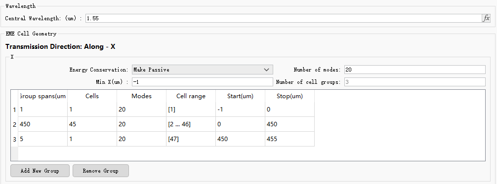
In general, because the waveguide cross-sectional structures at the fiber and chip facets are different, to accurately capture the transmission and reflection characteristics at the fiber/chip interface, one EME cell should be placed on each side of the interface. The S-parameter results in this example are calculated under the assumption of zero gap (direct contact) between the fiber and the chip facet, and can reflect the reflection characteristics at the interface. For packaging-level accuracy, the packaging environment around the fiber and chip should also be included in the simulation so that the S-parameter results can include the additional loss introduced by the packaging.
Regarding boundary conditions, perfect electric conductor (PEC) boundary conditions are usually used for tapered waveguide devices because the scattered light mainly propagates outward in the form of higher-order unbound modes, attenuates rapidly, and the light recoupled back into the fundamental mode is almost negligible. In this example, except for the Y-axis minimum boundary (Y axis min), which uses an anti-symmetric boundary condition, all other boundaries use PEC boundary conditions.
Simulation Results
FDE Optimization of Fiber Position
Open the attached edge_coupler_no_substrate.mpps project and run the edge_coupler_FDE.msf script. The script enables the FDE solver and performs simulations for models containing only the SMF-28 fiber and only the edge coupler, respectively, extracting the TE fundamental modes of both. It then calculates the overlap integral between the two fundamental modes and applies a spatial offset to the SMF-28 mode within a certain range to obtain the maximum overlap integral and the corresponding SMF-28 fiber position. As shown below, after position scanning, the maximum overlap integral between the two modes is 0.784.
The overlap before optimize position is 0.758635
After optimize position, the maximum overlap is 0.783964
The best location of SMF-28 is:
    x pos = 0.00 um,
    y pos = -0.05 um,
    z pos = -0.44 um
EME Optimization of Tapered Waveguide Length
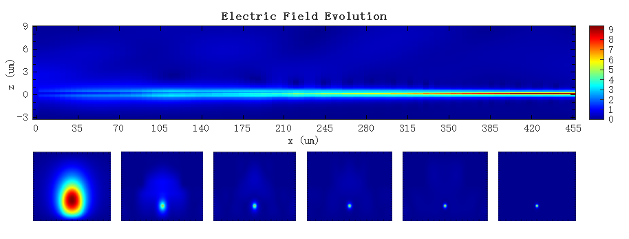
According to the FDE simulation results, adjust the fiber to the position with the highest coupling efficiency, and then run the edge_coupler_EME.msf script in the same project. This script disables the FDE solver and enables the EME solver, and runs an EME simulation that includes both the SMF-28 fiber and the edge coupler structure. After the script finishes, the EMEProfileMonitor monitor can be used to visually observe the evolution of the electric field. The results clearly verify the spot size converter (SSC) function of the edge coupler, that is, it can smoothly transition the larger mode field in the fiber and efficiently couple it into the sub-micron spot in the on-chip waveguide.
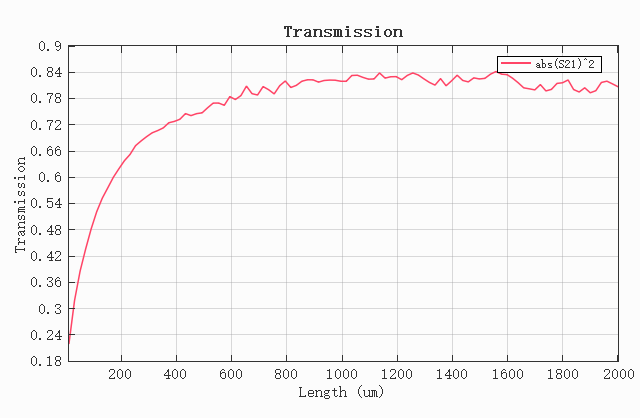
In addition, the script runs an EME propagation sweep, sweeping the length of cell group 2 from 10 μm to 2000 μm with 100 scan points. The results are shown below. When the length of the tapered waveguide is about 1550 μm, the coupling efficiency reaches its maximum.
References
[1] M. Papes, et al., "Fiber-chip edge coupler with large mode size for silicon photonic wire waveguides," Opt. Express, 24(5), 5026-5038 (2016).