

SimWorks Stack Solver (STACK) Settings
Optical Multilayer Solver #
The Optical Multilayer (STACK) solver is used to analyze the optical properties of one-dimensional multilayer thin-film structures. It divides the multilayer stack into a series of uniform layers along the propagation direction and uses the transfer matrix method (TMM) to calculate the transfer matrices at each layer interface and during propagation, thereby obtaining the reflectance, transmittance, field distribution, and other optical responses of the entire stack.
The STACK solver is particularly suitable for simulating planar multilayer devices such as anti-reflection coatings, high-reflection coatings, OLEDs, and thin-film solar cells. Compared with 3D FDTD simulation, the STACK solver requires no mesh generation and uses an analytical method with no numerical discretization error, achieving extremely fast computation while maintaining accuracy, making it ideal for parameter sweeps and optimization iterations.
STACK Solver Settings #
Select the STACK button in the Home tab, then click anywhere in the Composite Viewer to create a STACK solver. The edit properties window will pop up automatically; modify the STACK solver settings there to complete adding the STACK solver.
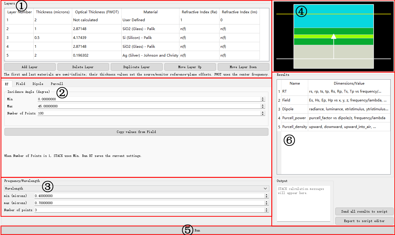
The STACK solver settings page is shown below. Unlike other solvers, the STACK solver does not have an independent simulation control panel. After configuring the simulation parameters in Area 1 to Area 3, you can preview the structure and source through Area 4, then click the Run in Area 5 to run the simulation. The simulation results and the solver's computation messages can be viewed or exported in Area 6. Detailed descriptions for each area will be provided in subsequent sections.
Layers #
The Layers table is used to define the detailed structure of the multilayer stack, including the thickness, material, and optical properties of each layer.
| Name | Description |
|---|---|
| Layer Number | Layer index. The first layer is the incident layer, and the last layer is the exit layer. |
| Thickness (microns) | Thickness in microns. For the first and last layers, the thickness is treated as semi-infinite, and the thickness value is used to set the offset of the source and monitor reference planes. |
| Optical Thickness (FWOT) | Optical thickness, calculated based on the center frequency. |
| Material | Material. Defaults to User Defined, and the refractive index can be set manually; it can also be selected from the material library. Note: If a material from the library is selected, the STACK solver will use interpolated data from the material database rather than multi-coefficient fit data. |
| Refractive Index (Re) | Real part of the material refractive index. |
| Refractive Index (Im) | Imaginary part of the material refractive index. |
The optical thickness is defined as follows:
FWOT=λn×d
where n is the real part of the material refractive index, d is the layer thickness, and λ is the central wavelength.
The Layers table provides the following operation buttons below:
| Name | Description |
|---|---|
| Add Layer | Add a new layer to the table. |
| Delete Layer | Delete the currently selected layer. |
| Duplicate Layer | Duplicate the currently selected layer. |
| Move Layer Up | Move the selected layer up. |
| Move Layer Down | Move the selected layer down. |
The STACK solver can visualize the settings in the Layers table and display the positions of the source and monitors. Note that if the source and monitors are placed inside an absorbing material (i.e., the imaginary part of the refractive index is nonzero), their positions will affect the reflection and transmission coefficients.
RT #
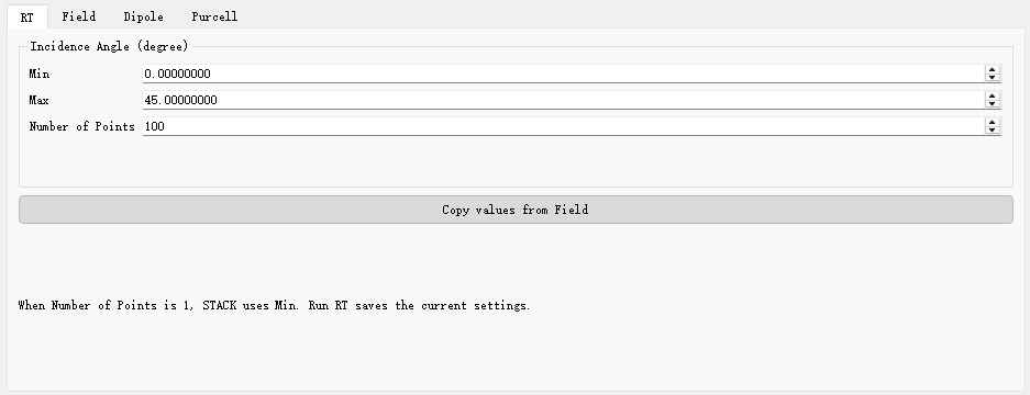
Calculates the reflectance and transmittance of a plane wave incident on the multilayer thin-film structure. The settings are as follows.
Incidence Angle #
| Name | Description |
|---|---|
| Min | Set the minimum incidence angle in degrees (°). |
| Max | Set the maximum incidence angle in degrees (°). |
| Number of Points | Set the number of points for the angle sweep. If the number of points is 1, the STACK solver will use the Min value for calculation. |
Additionally, the angle settings from the Field page can be copied via the Copy values from Field button.
Field #
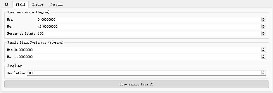
Calculates the electric and magnetic field distributions inside the multilayer thin-film structure. The settings are as follows.
Incidence Angle #
| Name | Description |
|---|---|
| Min | Set the minimum incidence angle in degrees (°). |
| Max | Set the maximum incidence angle in degrees (°). |
| Number of Points | Set the number of points for the angle sweep. |
Result Field Positions #
| Name | Description |
|---|---|
| Min | Set the minimum value of the output result along the source propagation direction (z direction) in microns (µm). |
| Max | Set the maximum value of the output result along the source propagation direction (z direction) in microns (µm). |
Sampling #
| Name | Description |
|---|---|
| Resolution | Set the resolution of the output result along the source propagation direction (z direction). Must be ≥ 2. |
Additionally, the angle settings from the RT page can be copied via the Copy values from RT button.
Dipole #
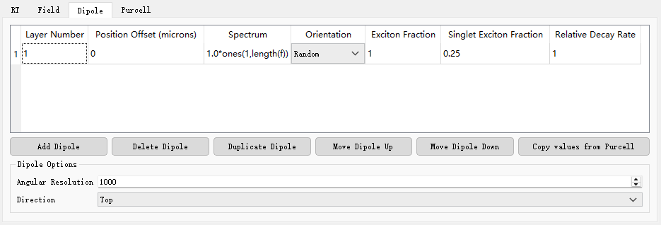
Calculates the angular radiance, luminance, and CIE 1931 chromaticity coordinates for electric dipoles in an isotropic or z-birefringent planar multilayer film stacking structure. The settings are as follows.
| Name | Description |
|---|---|
| Layer Number | Layer index where the dipole is located. |
| Position Offset (microns) | Position offset of the dipole relative to the bottom of the layer, in microns (µm). |
| Spectrum | Dipole spectrum. The spectrum is treated as a power intensity distribution and integrated using midpoint integration in wavelength. The photon probability distribution is calculated by normalizing dipole_spec/f. The matrix size is N_dipoles × length(f), where N_dipoles is the number of dipoles and length(f) is the length of the frequency array. |
| Orientation | Dipole orientation. Defaults to Random; can be Random, Vertical, or Horizontal. |
| Exciton Fraction | Exciton fraction. Describes the proportion of exciton recombination in dipole radiation. Default is 1, meaning every carrier results in an exciton. |
| Singlet Exciton Fraction | Singlet exciton fraction. Describes the proportion of singlet excitons in total excitons. Default is 0.25, meaning there are 3 spin triplets per spin singlet. |
| Relative Decay Rate | Relative decay rate. Used to set the initial decay rate of the dipole. Default is 1, meaning every singlet exciton results in a photon and there is no contribution from non-radiative decay processes. |
The table provides the following operation buttons below:
| Name | Description |
|---|---|
| Add Dipole | Add a new dipole to the table. |
| Delete Dipole | Delete the currently selected dipole. |
| Duplicate Dipole | Duplicate the currently selected dipole. |
| Move Dipole Up | Move the selected dipole up. |
| Move Dipole Down | Move the selected dipole down. |
| Copy values from Purcell | Copy the dipole settings from the Purcell page. |
Dipole Options #
| Name | Description |
|---|---|
| Angular Resolution | Far-field emission angle resolution, used to set the calculation accuracy of the dipole radiation direction. |
| Direction | Far-field half-space. Defaults to Top; can be Top or Bottom. |
Purcell #
Calculates the Purcell factor and far-field emitted power density for electric dipoles in an isotropic or z-birefringent planar multilayer film stacking structure. The settings are as follows.
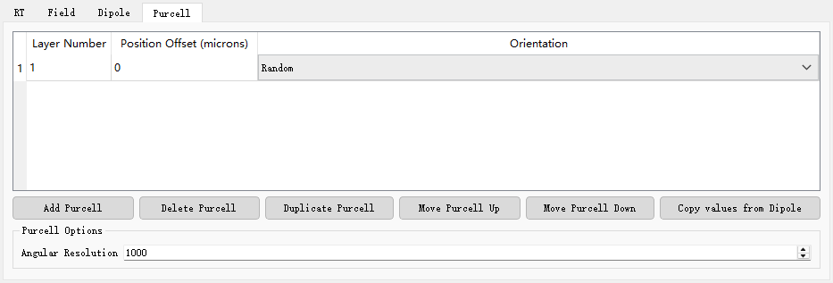
| Name | Description |
|---|---|
| Layer Number | Layer index where the dipole is located. |
| Position Offset (microns) | Position offset of the dipole relative to the bottom of the layer, in microns (µm). |
| Orientation | Dipole orientation. Defaults to Random; can be Random, Vertical, or Horizontal. |
The button functions below the table are the same as those on the Dipole page.
Purcell Options #
| Name | Description |
|---|---|
| Angular Resolution | Far-field emission angle resolution, used to set the calculation accuracy of the dipole radiation direction. |
Frequency/Wavelength #
Sets the frequency or wavelength range and number of points for the solver calculation.

| Name | Description |
|---|---|
| Frequency/Wavelength | Select the input parameter type: Frequency or Wavelength. |
| min (THz) | Set the minimum frequency in terahertz (THz). |
| max (THz) | Set the maximum frequency in terahertz (THz). |
| min (microns) | Set the minimum wavelength in microns (µm). |
| max (microns) | Set the maximum wavelength in microns (µm). |
| Number of points | Set the number of sampling points. |
Results and Output #
After setting up, click the Run button at the bottom of the page to perform the simulation. The calculation results can be viewed in the Results table, and the Output area displays the calculation messages of the STACK solver.
You can right-click on a result of interest to view it, send it to the script workspace, or directly view the data table of the result. In addition, clicking Send all results to script sends all results to the script workspace; clicking Export to script editor exports the script that builds this STACK simulation to the script editor.