

Vertical Photodetector
Preface
A vertical photodetector is a core optoelectronic device that converts optical signals into electrical signals. Its typical structure consists of a germanium ( ) absorption layer integrated above a silicon ( ) waveguide. Light is vertically coupled from the silicon waveguide into the layer through a tapered coupling structure and absorbed, generating electron-hole pairs, which are separated under the built-in electric field to form a photocurrent. Compared with traditional surface-incident photodetectors, vertical photodetectors offer advantages such as compatibility with silicon photonic integrated circuits, high absorption efficiency, fast response, and ease of large-scale integration, and have broad application prospects in optical interconnects, optical communications, data centers, and other fields. Based on reference [1], this example simulates a vertical photodetector, using the eigenmode expansion (EME) solver to optimize the device dimensions and the finite-difference time-domain (FDTD) solver to calculate parameters such as the photo-generated carrier generation rate.
Simulation Settings
Structure Model
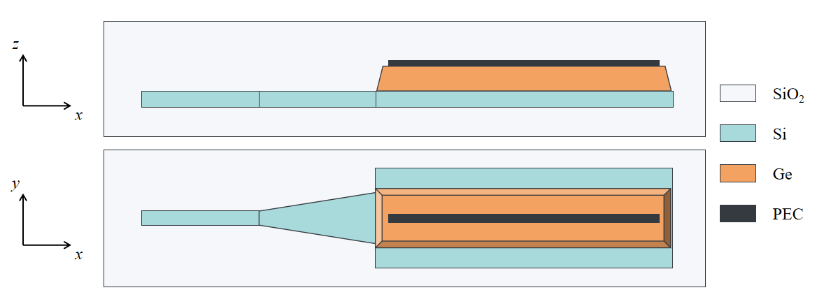
As shown in the figure above, the vertical photodetector consists of six parts: an input waveguide, a tapered waveguide, a waveguide, a absorption layer, a perfect electric conductor ( ) layer, and a silicon dioxide ( ) cladding. The incident light is coupled into the waveguide through the input waveguide and the tapered waveguide; above the waveguide is the absorption layer, which absorbs light and generates electron-hole pairs; a layer covers the absorption layer and serves as the cathode electrode, which is treated as an ideal conductor in the optical simulation. The above five structures are all embedded in the cladding.
The device length affects the absorption performance, so the optimal device length needs to be determined. For the FDTD solver, calculating the absorption as a function of length is very time-consuming. Since the structure is uniform in cross-section along the propagation direction except for the tapered transition region, the EME solver can be used to quickly calculate the optimal device length, as shown in the figure below. The entire structure is divided into four cell groups along the propagation direction. Cell group 2 is the tapered transition region of the absorption layer, where multiple cells are set to accurately resolve the structural variation, while the other cell groups each contain only one cell.
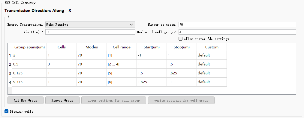
In addition, to reduce the computational cost of the simulation, the tapered waveguide is not included in the EME simulation. Instead, the width of the input waveguide is directly set to the width of the wider end of the taper, which is equivalent to assuming that all the incident light is coupled into the fundamental mode of the wide waveguide after passing through the tapered waveguide. This is an approximation that neglects the coupling of part of the optical power into higher-order modes of the wide waveguide by the tapered waveguide. This is because the EME length sweep mainly focuses on the trend of the total absorbed power in the absorption layer as a function of device length, rather than the mode in which the light is absorbed. Therefore, neglecting the tapered waveguide effectively reduces the simulation complexity and improves the calculation speed.
Simulation Results
EME Optimization of Device Length
Open the attached vertical_photodetector_EME.mpps project and run the vertical_photodetector_EME.msf script. The script sequentially modifies the length of the fourth cell group in the EME solver, sweeping from to , with a total of 10 points. After each modification, the EME propagation calculation is performed again to extract the refractive index and electric field distribution, calculate the absorbed power density within the absorption layer, and then integrate over space to obtain the normalized absorbed power. Finally, the script plots the curve of absorbed power versus device length to determine the optimal device length, as shown below.
It can be seen from the figure that when the device length increases from to , the absorbed power rises rapidly from about to about , reaching about of the saturation value ( ) . The data show that when the device length is doubled (from to ) , the absorption increases only from to , an increase of less than . From the perspective of FDTD simulation, this small performance improvement is not enough to offset the significant increase in computation time caused by the larger size. Based on the trade-off between computational efficiency and simulation accuracy, the length of the absorption layer is set to in the subsequent FDTD simulation.
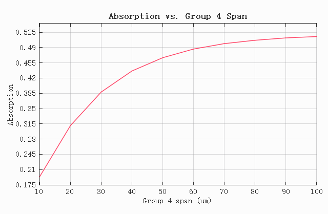
In addition, the absorption saturation value is only , mainly because the discretization accuracy of cell group 2 is relatively low. Cell group 2 is the tapered transition region of the absorption layer, where only 3 cells are set, which is equivalent to a staircase approximation of the tapered region, resulting in a lower final result. Increasing the number of cells in cell group 2 can effectively increase the absorption saturation value, but this does not affect the overall trend of absorption versus length. Setting the simulation length of the absorption layer to in FDTD still achieves relatively high absorption while reducing simulation time.
FDTD Calculation of Photo-Generated Carrier Generation Rate
Open the attached vertical_photodetector_FDTD.mpps project. The simulation length of the absorption layer has been set to based on the EME optimization results. After the simulation is completed, the Generation_rate analysis group reads the monitor data, calculates the absorbed power density from the electric field distribution and the material refractive index, and further obtains the photo-generated carrier generation rate. The generation rate is averaged along the propagation direction ( direction) and saved as a vpd_generation_rate.mat file, which can be used for electrical simulation.
The script also calculates key parameters such as the short-circuit current density and the maximum generation rate, and plots the absorption power versus wavelength as well as the spatial distribution of the generation rate on three typical cross-sections, as shown below. At a wavelength of , the absorption is about , which is close to the absorption ratio obtained from the EME optimization ( ) . When the input power is normalized to , the total photocurrent generated within the entire simulation volume is , the short-circuit current density is , and the maximum generation rate within the absorption layer is .
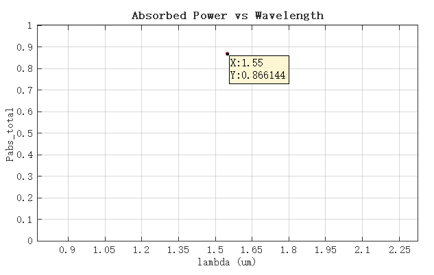
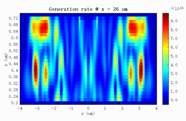
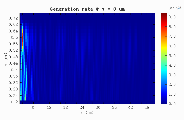
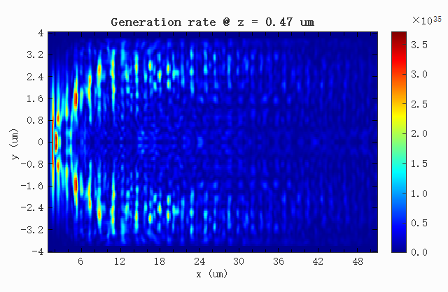
The above results show that the spatial distribution of the photo-generated carrier generation rate calculated by FDTD is reasonable, and the absorption spectrum has high absorption efficiency at the operating wavelength, which can provide an accurate carrier generation rate for subsequent electrical simulations.
References
[1] T. Y. Liow, et al. "Silicon Modulators and Germanium Photodetectors on SOI: Monolithic Integration, Compatibility, and Performance Optimization," IEEE J. Sel. Top. Quantum Electron., 16(1), 307-315 (2010).