Focusing Grating Coupler
Preface
In many fields of data communication, high-speed optical interconnection technology is essential for huge data exchange, and thus the integration of optical interconnection has been a hot research topic in recent years. The leading candidate technology is silicon photonic circuits due to its superior performance, low cost, and monolithic integration with other optoelectronic components. One important issue of silicon photonic circuit is an interface between integrated waveguide devices and optical fibers or free-space optics. Grating couplers have the advantages of easy fabrication, high flexibility, and large alignment tolerance, which makes them the most important solution to solve the coupling issues. In this example, inspired by the work of and his colleagues[1], we simulate a focusing grating coupler to study its coupling capability.
Simulation settings
Device introduction
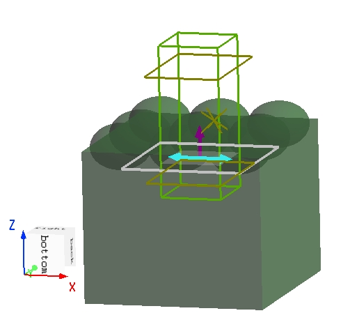
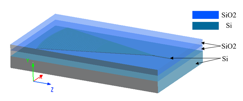
The focusing grating coupler used in this example is based on a shallow-etched silicon substrate with a waveguide layer, cladding on both the top and bottom, and the lowest substrate material is still , as shown in the figure above. The direction is the optical transmission direction, and the thickness direction of the optical waveguide is the direction. Since the structure is symmetric in the direction and the light source is anti-symmetric in the direction, we use the Anti-Symmetric boundary condition in the direction.
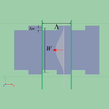
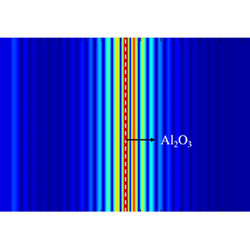
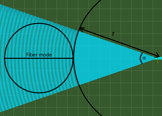
A confocal grating is used for the coupling grating part, and its process parameters (waveguide thickness, buried oxygen layer thickness, substrate thickness, cladding thickness, and shallow etch depth) are specified based on IME, and the grating period, duty cycle, and taper are designed referring to paper[1:1], as shown in the figure below. The grating itself focuses light into a silicon wire waveguide of width , where the taper has a tensor angle of and a of . In the design, the grating pattern is a concentric circular line, with the center of the circle at the apex of a wedge intersecting the waveguide.
| Variables | Period/ | Duty |
|---|---|---|
| Value | 0.67 | 0.53 |
Source
The incident light received by the focusing grating is typically emitted from a step-index-single-mode fiber. After leaving the fiber, the light directly enters the glass cladding at the top of the grating structure. Since the output light from the step-index single-mode fiber can be approximated as having a Gaussian field distribution, the step-index single-mode fiber itself is not modeled in this simulation project. Instead, the output light from the fiber is replaced with a Gaussian source. Therefore, when setting up a Gaussian source in the software, the following points should be noted:
- The waist size of the
Gaussiansource should match the actual core size of the fiber being used. - The position of the
Gaussiansource's waist surface represents the contact point between the fiber and the top cladding of the grating, so the background material at the light source location should be set to Silica(glass).
Simulation results
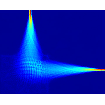
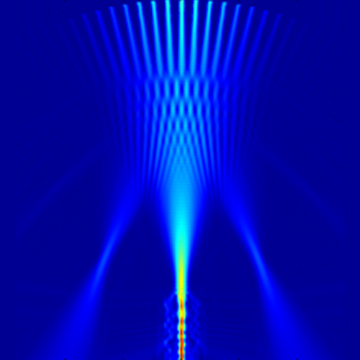
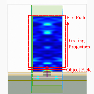
The electric field distribution at a wavelength of obtained in the FDFP monitor placed inside the focusing grating coupler is shown in the figure below. Clearly, the free-space light from the Gaussian source is coupled by the grating into the silicon wire waveguide on the right.

The figure displays the transmittance distribution with wavelength obtained from the 'FDFP' monitor in the silicon wire waveguide when the Gaussian light source is away from the silicon wire waveguide. It is evident that the focusing grating coupler achieves a maximum transmittance of at a wavelength of .

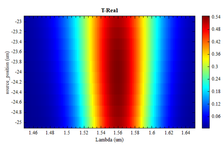
Parameter analyses
The project includes a parameterized sweep that scans the Gaussian source from to away from the silicon wire waveguide in the optical propagation direction. After the sweep, you can obtain the distribution of transmittance T varying with the position of the light source. The figure shows that the maximum transmittance of the focusing grating coupler is achieved at a wavelength of when the light source is away from the silicon wire waveguide, with a T value of .