Focusing Polarization Splitting Grating Coupler
Preface
With SOI platform widely used in the integrated optics, the grating coupler has emerged as crucial components in silicon nanophotonics by virtue of its advantages of easy processing, easy alignment and easy integration. The polarization state of light in optical fibers is often difficult to determine, at the same time, the grating coupler is highly sensitive to the polarization of light, and there are significant differences in coupling efficiency for different polarization states of light. Therefore, addressing the coupling issue between optical fibers and waveguides has become a prominent research focus in recent years. Polarization splitting grating couplers can simultaneously achieve polarization beam-splitting and light coupling functions, which enables the vertical grating coupling between fibers and SOI platform for various polarization states. This approach represents one of the most optimal solutions to tackle this issue.
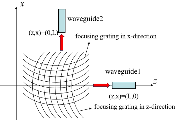
Based on the work of Frederik et al.[1], a two-dimensional (2D) focusing polarization splitter grating coupler is constructed. The standard 2D focusing polarization splitting grating coupler can be considered as the approximate superposition of two 1D focused grating couplers placed orthogonally. The incident direction of the fiber is perpendicular to the plane of the grating coupler. After polarization selection by the grating coupler, the incident light is focused into two different output ports, as shown in the following figure.
Simulation settings
Device introduction
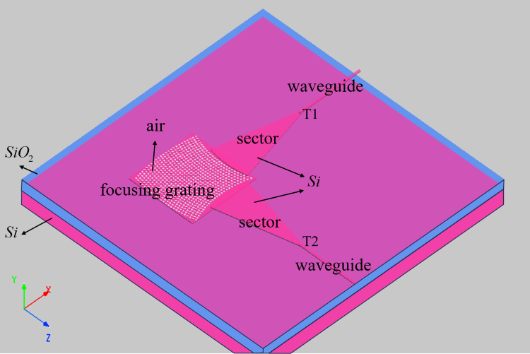
The simulation structure in 3D FDTD is shown in the following figure. It is effective to add a sector structure between the grating coupler and the output waveguide to reduce the coupling loss. The entire grating coupler is based on the SOI platform that has a three-layer structure. The bottom layer is , the middle layer is , and the upper layer is placed with optical waveguide devices. In this example, the grating coupler is composed of a series of air holes etched on the substrate. The center of the circular hole is located at the intersection of two 1D focusing grating lines. The relevant parameters are shown in the table below according to ref[1:1].
| name | size |
|---|---|
| Waveguide Length | |
| Waveguide Depth | |
| Hole Depth | |
| Hole Radius | |
| L |
Source
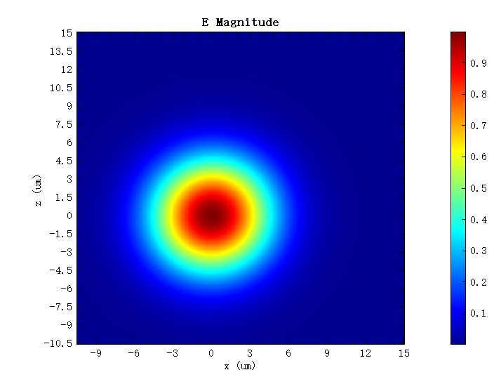
In this case, Gaussian source is used to simulate the fundamental mode in optical fiber. The source is tilted to minimize reflection. The waist radius and tilt angle of the Gaussian light source are set as follows. The electric field of the source is shown in the following figure.
| name | size |
|---|---|
| Waist Width | |
| Angle Theta | |
| Angle Phi | |
| Linearly Polarization |
Simulation results
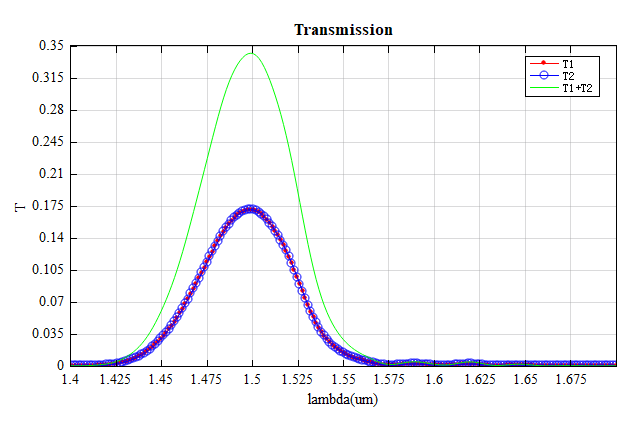
After opening and running the attached project, it can be observed that the light is equally divided into two output ports at the 1.5.

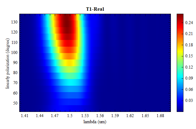
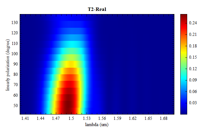
The following results can be obtained by running the script focusing_grading_plot. In the graph, the transmittance of both output ports is equal, and the total of T1 and T2 exceeds 0.34.
Parameter analyses
By running parameters sweep, we can observe the relation between the transmittance of the two ports and the polarization angle of the source. As the polarization angle shifts from 45 degrees to 135 degrees, the light switches from one output port (e.g.,T2) to the other (e.g.,T1).