Bandstructure of 2D Triangular Lattice
Preface
In 2D photonic crystals, different lattice types possess completely different band structures. The base settings in FDTD simulations vary with the different lattice types. In this case, a 2D triangular-lattice photonic crystal formed by air cylinders arranged in parallel in the medium is constructed, and its bandstructure is calculated. Based on the following example, some special settings and precautions for FDTD simulation of non-rectangular lattice photonic crystals are introduced.
Simulation settings
Device introduction
The FDTD solver is used to analyze the bandstructure of a triangular-lattice photonic crystal consisting of periodically arranged air cylinders in a homogeneous medium. Similar to the 2D square-lattice photonic crystal, the periodic arrangement of air cylinders in homogeneous media also realizes the periodic refractive index distribution, forming a photonic bandgap, which prevents some specific frequencies of light from entering the structure. In this photonic crystal, the refractive index of the dielectric material is 2, the radius of the periodically arranged air cylinder is 200 nm, and the lattice spacing of the triangular-lattice is 500 nm. For such triangular-lattice photonic crystals with non-rectangular lattice structure, at least two lattice cells are required in the FDTD simulation region.
Device construction
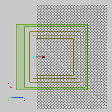
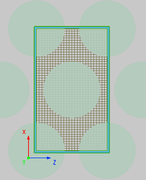
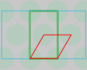
The simulation setup of this case is similar to the case of Bandstructure of 2D Square Lattice, and will not be repeated here. Please download the attached file for detailed information. Because the shape of the FDTD simulation region is limited by the rectangular mesh, the non-rectangular lattice structure can not be simulated with only one complete lattice periodic cell like the rectangular lattice structure. For photonic crystals with 2D triangular lattice or other non-rectangular lattice, the overall lattice structure can only be divided into rectangular regions suitable for FDTD solver. As shown in the figure below, the triangular lattice structure can be seen as a square lattice repeatedly arranged by the rectangular structure inside the green wireframe. Therefore, the simulation region is selected to be consistent with the wireframe, and the structure in it is simulated.
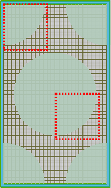
It should be noted that each unit of photonic crystal structure must be partitioned in the same method and size. Ensure the uniformity and periodicity of the refractive index distribution, so as to avoid inaccurate calculation results. As shown in the following figure (within the dotted box), the mesh distributions at the corresponding positions of different structural elements are compared. It is obvious that each circular structure region is partitioned in the same way. This requires that the number of grids in the simulation area must be even, and the grid is symmetrically distributed about the center coordinate axis of the simulation area (On the solver Advanced Settings page, select the 'force symmetric X/Z mesh' option under 'Mesh Generation' to force the construction of a mesh that is symmetric about the X/Z axis.).
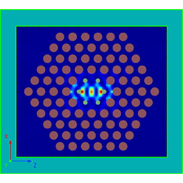
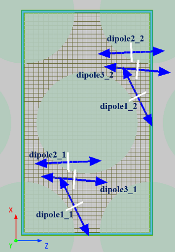
For the model with multiple unit cells in the simulation region, in order to avoid the artificial region folding, we must have a matching dipole source in each unit cell, and each set of matched dipole sources must have exactly the same position in the unit cell. The phase difference between the dipole sources must satisfy the formula , where is the wave vector of the simulation and is the position-varying vector of the two dipole sources. The built-in script of the analysis group 'Dipole Clouds' will complete the construction of such a dipole array by simply setting the variable values in the analysis group according to the photonic crystal. As shown in the figure, three sets of matching dipole sources are constructed.
Simulation results
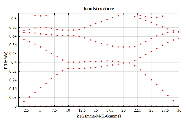
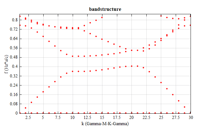
Download and open the attached file triangular_2D.mpps. After running all parameter sweeps, run the script file (triangular_2D.msf) to obtain the sweep results and draw the bandstructure diagram in TE mode, as shown below.
The bandstructure in TM mode can be calculated by changing the polarization type in the solver properties, as shown below.