
Rigorous Coupled‑Wave Analysis (RCWA) Solver Settings
RCWA Settings #
This section introduces the various parameter settings of the RCWA solver.
The Rigorous Coupled‑Wave Analysis (RCWA) solver is a semi‑analytical simulation tool used to analyze the optical response of multilayer structures with in-plane periodic patterns under plane-wave incidence, including reflectance, transmittance, diffraction efficiency, and internal field distributions.
The RCWA solver is particularly suitable for analyzing and designing devices with periodic subwavelength structures, such as diffraction gratings, metasurfaces, photonic crystal slabs, and waveguide gratings. Its fundamental principle is to analytically solve Maxwell's equations for each layer in the Fourier domain, where the Fourier mode wave vectors are the K vectors. Increasing the number of K vectors improves simulation accuracy. For structures with sharp boundaries or high refractive index contrasts, it is recommended to increase the number of K vectors appropriately and perform convergence testing. After sufficient convergence, RCWA results are highly consistent with FDTD. For periodic multilayer structures, the RCWA solver can serve as an effective alternative to FDTD.
Among the optical simulation tools in SimWorks, RCWA, FDTD, and the STACK script functions each have their own strengths and are suited for different application scenarios:
| Solver/Method | Algorithm Principle | Applicable Scenarios | Features and Limitations |
|---|---|---|---|
| FDTD | Finite‑Difference Time‑Domain method, directly discretizing and solving Maxwell's equations in the time domain | Arbitrary complex geometries (both non‑periodic and periodic) | High versatility and flexibility; broad‑bandwidth results can be obtained in a single simulation; however, for large‑period structures requiring high‑resolution detail, the simulation becomes computationally heavy and time‑consuming. |
| RCWA | Semi‑analytical method, analytically solving Maxwell's equations for each layer in the Fourier domain | Multilayer structures with in‑plane periodic patterns | Significantly faster than FDTD, relatively simple setup; accuracy depends on the number of K vectors, and the results after convergence are highly consistent with FDTD. |
| STACK script functions | Analytical transfer‑matrix method, directly solving reflection and transmission of multilayer films | Multilayer film structures with uniform geometry (no in‑plane patterns) | Fastest simulation speed, invoked via script functions such as stackrt and stackfield; only applicable to uniform layered structures without in‑plane patterns; as an analytical method, it has no numerical discretization errors and offers the highest accuracy. |
In practice, the most suitable method should be chosen based on the geometric characteristics and physical requirements of the structure: STACK script functions are preferred for uniform multilayer film structures; RCWA is preferred for multilayer structures with in‑plane periodic patterns; and FDTD is preferred for arbitrarily complex structures that are not large-period.
RCWA Solver Settings #
In the Home tab, click the RCWA button, then click anywhere in the composite viewer window to create an RCWA solver. The solver settings can then be modified in the automatically opened Edit Property window, completing the addition of the RCWA solver.
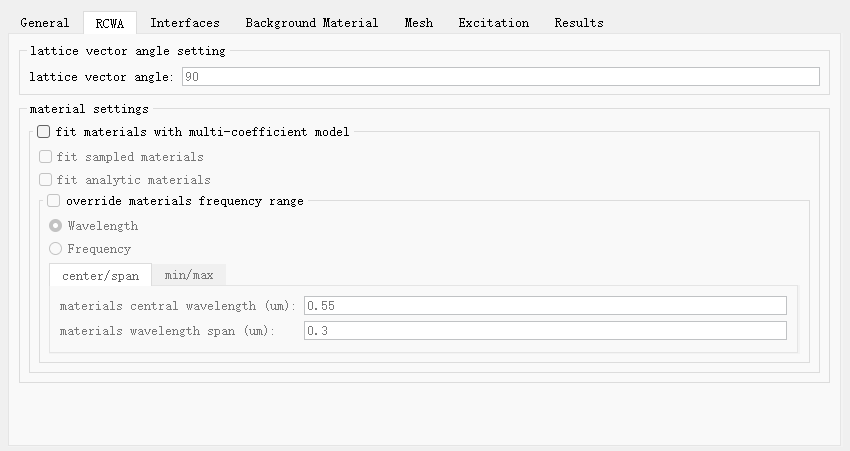
The RCWA solver property page is shown below, with detailed explanations provided in the following sections.
General Settings #
The General tab configures the solver's simulation space, including the propagation axis, propagation direction, and geometric dimensions of the simulation region.
Propagation Axis and Direction #
| Name | Description |
|---|---|
| Propagation axis | Sets the coordinate axis along which the electromagnetic wave propagates; options are x, y, or z. The normal direction of the structure is typically chosen as the propagation axis. |
| Propagation direction | Sets the wave propagation direction along the propagation axis; options are Forward (positive direction), Backward (negative direction), or both (both directions simultaneously). |
Simulation Region Geometry #
| Name | Description |
|---|---|
| x/y/z pos | Sets the geometric center coordinates of the solver's simulation region. |
| x/y/z span | Sets the extent (total length) of the solver's simulation region along the three coordinate axes. |
RCWA Settings #
This tab contains core settings specific to the RCWA algorithm, used to control lattice geometry, material models, and algorithmic behavior.
Lattice Vector Angle #
| Name | Description |
|---|---|
| Lattice vector angle | Sets the angle (in degrees) between the lattice basis vectors. For non‑orthogonal lattices, the angle between the two basis vectors must be specified to accurately describe the unit cell geometry. |
Material Fitting Settings #
These options control how material dispersion models are fitted; the following options can be checked:
| Name | Description |
|---|---|
| Fit materials with multi‑coefficient model | Uses a multi‑coefficient model to fit the material, improving the accuracy of material dispersion characteristics. |
| Fit sampled materials | Fits sampled material data (e.g., experimental data imported from files). |
| Fit analytic materials | Fits analytical material models (e.g., Drude, Lorentz, etc.). |
Override Materials Frequency Range #
When Override materials frequency range is checked, users can manually specify the frequency/wavelength range used for material property calculations, overriding the material's default range.
| Name | Description |
|---|---|
| Wavelength / Frequency | Toggles the unit system; options are wavelength or frequency. |
| Center / Span | Sets the center value and total span (range width). |
| Min / Max | Directly sets the minimum and maximum values of the range. |
Interface #
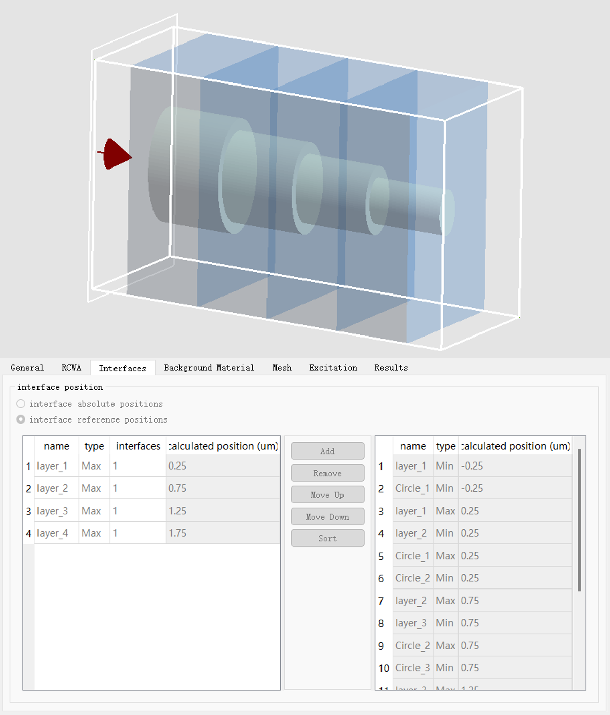
The Interface tab defines the positions of layer interfaces within the structure, supporting two positioning methods.
| Name | Description |
|---|---|
| Interface absolute positions | Directly specifies the position of each interface by entering absolute coordinate values. |
| Interface reference positions | Defines interface positions based on the reference positions of geometric objects; when the geometric object positions change, the interface positions automatically update accordingly. |
Background Material #
In the Background Material tab, a Background Material dropdown menu is provided for users to select the background material.
| Name | Description |
|---|---|
| Background material | Background material library; users can select materials from the Optical Material library and set them as the background material. |
After selecting a background material, the relevant material information (Name, Type, Last modified, etc.) is displayed simultaneously.
Mesh #
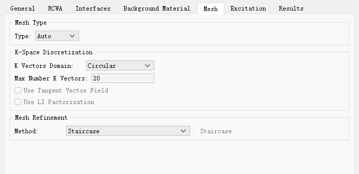
The Mesh tab provides mesh and K‑space discretization settings for the solver.
Mesh Type #
| Name | Description |
|---|---|
| Mesh type | Options are auto or custom. auto is suitable for most typical simulations; custom allows users to manually adjust mesh parameters for higher simulation accuracy in specific scenarios. |
K‑Space Discretization #
| Name | Description |
|---|---|
| K vectors domain | The shape of the range used to select Fourier harmonics in K‑space can be chosen as circular or rectangular, which affects the simulation accuracy and computational load. |
| Max number of K vectors | Enabled when circular is selected; the maximum number of K vectors. A larger number improves accuracy but increases computation time. |
| Max number of ku / kv | Enabled when rectangular is selected; the maximum number of K vectors in the u and v directions in K‑space, controlling the Fourier component accuracy in each direction. |
For detailed Mesh refinement settings, please refer to the Mesh documentation.
Excitation #
The Excitation tab sets the incident wave angle and frequency parameters.
Incident Angle #
| Name | Description |
|---|---|
| Incident angle | Configuration mode for the incident angle; options are single, table, or range. |
Single Mode:
| Name | Description |
|---|---|
| Angle theta (degrees) | The polar angle θ of the incident light (in degrees), i.e., the angle between the incident direction and the normal direction of the structure. |
| Angle phi (degrees) | The azimuthal angle ϕ of the incident light (in degrees), i.e., the rotation angle of the incident direction within the plane. |
Table Mode:
Multiple angle combinations can be added via a table, with each row specifying theta (degrees) and phi (degrees). The simulation will compute all combinations sequentially.
Range Mode:
| Name | Description |
|---|---|
| Theta spacing | Sampling interval method for θ; options are linear or cosine. |
| Minimum theta / maximum theta (degrees) | The minimum and maximum values of θ. |
| Minimum phi / maximum phi (degrees) | The minimum and maximum values of ϕ. |
| Theta points / phi points | The number of sampling points in the θ and ϕ directions. |
Frequency Settings #
This option configures the frequency/wavelength sampling points used in the simulation.
| Name | Description |
|---|---|
| Central wavelength (μm) | The center wavelength of the wavelength range, in micrometers. |
| Wavelength span (μm) | The total span of the wavelength range, in micrometers. |
| Minimum wavelength / maximum wavelength (μm) | Directly specifies the minimum and maximum values of the wavelength range. |
| Wavelength points | The number of sampling points within the specified wavelength range; more points yield higher frequency resolution. |
| Edit complicated settings | Click to expand more frequency‑related detailed options (e.g., switching frequency units, etc.). |
Results #
The Results tab controls the types of data output after the simulation completes. Users can check the following options as needed:
| Name | Description |
|---|---|
| Report index | Outputs refractive index distribution information. |
| Report grating orders | Outputs information on each diffraction order (grating orders), including order numbers and their corresponding K vectors. |
| Report grating power | Outputs the power distribution of each diffraction order (i.e., diffraction efficiency of each order). |
| Report grating characterization | Outputs comprehensive characterization data of grating properties (e.g., polarization conversion efficiency, etc.). |
| Report field amplitudes | Outputs the electromagnetic field amplitude distribution, which can be used for further post‑processing analysis. |