
PN Junction Diode
Preface
A PN junction diode is a two-terminal device formed by the contact between a p-type semiconductor and an n-type semiconductor. Its core principle is that the PN junction forms a depletion region and a built-in voltage under thermal equilibrium, thereby exhibiting unidirectional conductivity. When a forward bias is applied, the barrier is lowered and the diffusion current grows exponentially; under reverse bias, the barrier is raised and only a small reverse saturation current exists. Compared with traditional vacuum tubes, PN junction diodes offer advantages such as small size, low power consumption, fast response, and ease of integration, and are widely used in rectification, switching, voltage regulation, photodetection, and other fields. This example uses the finite-difference charge transport (FDCharge) solver to model and simulate an ideal silicon PN junction diode, successfully obtaining key parameters including the band structure, built-in voltage, depletion region width, current-voltage characteristics, and junction capacitance, and verifying the consistency between the simulation results and the analytical model.
Simulation Settings
Structure Model
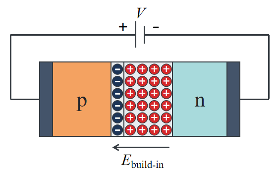
The PN junction diode is composed of silicon (Si) and aluminum (Al). Si is the semiconductor substrate of the device and the core medium for all carrier generation, transport, and recombination calculations; Al serves as the electrodes, forming the emitter and the base, respectively. To establish a built-in electric field, the entire Si region is uniformly doped with an N-type dopant (nepi), and a P-type dopant (pwell) is introduced below the emitter to control the carrier transport behavior, as shown in the table below.
| Doping Region | Doping Type | Concentration |
|---|---|---|
| nepi | n | |
| pwell | p |
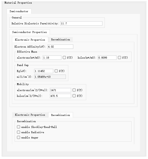
In this example, an ideal PN junction diode is simulated. In the material settings, the semiconductor uses defect-free Si_ideal, neglecting recombination mechanisms such as SRH recombination, Auger recombination, and Radiative recombination. The specific parameters and settings are shown in the figure below.
Simulation Results
Band Structure
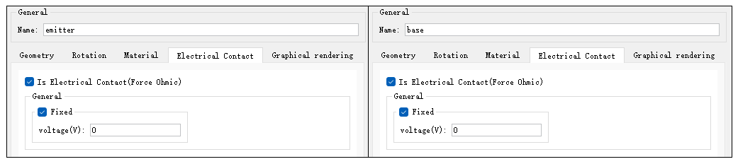
Before extracting the built-in voltage and the depletion region width, the PN junction must be brought into thermal equilibrium. Open the attached PN_junction_diode.mpps project and set both the emitter and base voltages to 0 V, i.e., no external bias, as shown in the figure below. At this point, the Fermi level of the device remains flat throughout the structure, and the band bending is entirely caused by the built-in electric field.
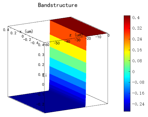
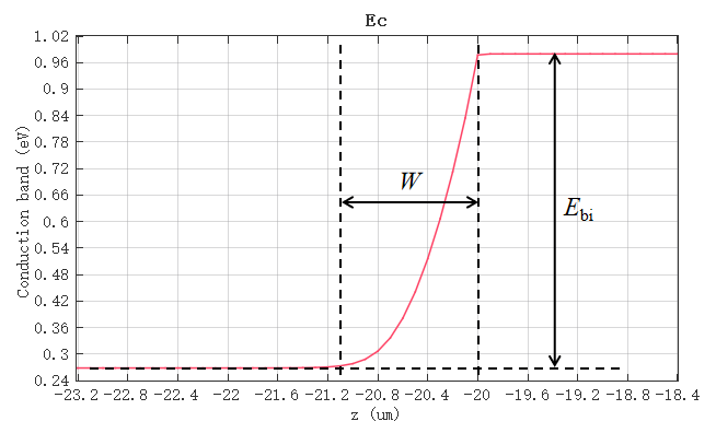
Run the simulation at zero bias. After the simulation, the band structure of the silicon substrate can be viewed in FDCharge::Charge Monitor::Bandstructure, including the conduction band (), the valence band (), and the intrinsic Fermi level (). Run the PN_junction_diode_equilibrium.msf script, which will plot , as shown below. It can be seen that the band remains flat in the neutral regions of the p-type and n-type regions, while significant band bending occurs in the depletion region. The total height of the band bending corresponds to the built-in voltage (), and the width of the bending region corresponds to the depletion region width ().
Built-in Voltage
The built-in voltage is defined as the difference between two energy levels in the n-type and p-type materials, expressed in eV. The built-in voltage already exists in the absence of an external voltage and does not produce a current. For a PN junction with ideal ohmic contacts, the built-in voltage is independent of the junction distribution. Assuming that the distance between the junction and the contacts is sufficient to establish local thermal equilibrium in the p-type and n-type regions, the built-in voltage can be determined by:
where is the Boltzmann constant, is the temperature, is the elementary charge, is the acceptor concentration in the p-type region, is the donor concentration in the n-type region, and is the intrinsic carrier concentration.
According to the simulation settings, , , , and . Substituting these into the above equation and taking , the theoretical value of the built-in voltage is approximately . The PN_junction_diode_equilibrium.msf script calculates the simulated built-in voltage as , as shown below, which agrees well with the theoretical value.
Depletion Region Width
When a abrupt junction is formed, the depletion region width can be predicted using the full depletion approximation:
where is the permittivity of the material. This expression is based on the following assumptions:
- The dopants are fully ionized;
- The junction is an abrupt junction;
- The carrier concentration in the space charge region is neglected ( and ).
In this example, , and the space charge layer is mainly distributed on the more lightly doped side, so the above expression can be simplified to:
In the simulation, , , , and . Substituting these into the above equation gives . The PN_junction_diode_equilibrium.msf script extracts and plots the conduction band energy, as shown in the figure, and also calculates the simulated depletion region width as . The difference between the theoretical and simulated values arises because the full depletion approximation is not sufficiently accurate: electrons and holes still exist within the space charge layer, and their concentrations are quite significant near the edges of this region, compensating the ionized dopant charges and thereby broadening the space charge layer.
Current-Voltage Characteristics
Assuming that recombination in the space charge region can be neglected, the diode equation can be derived based on the description of carrier injection current through the PN junction:
where is the junction area, is the applied voltage, are the diffusion coefficients, are the diffusion lengths, and is the reverse saturation current, expressed in terms of the minority carrier hole concentration in the n-type region and the minority carrier electron concentration in the p-type region.
Run the PN_junction_diode_iv.msf script to obtain the forward current-voltage characteristics of the diode. The script sets the emitter bias from 0.05 ~ 0.5 V, automatically runs the simulation to extract and plot the emitter current , and sets the y-axis scale to logarithmic, with the results shown below.
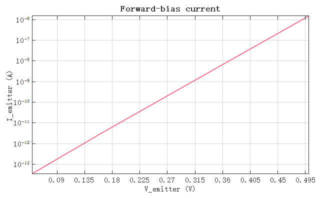
When the emitter bias is positive, the diode is forward-biased and the current grows exponentially with the bias:
where is the ideality factor. Taking the logarithm of the above equation shows that in logarithmic coordinates , i.e., the slope of the curve should be constant, which is consistent with the theoretical result.
Junction Capacitance
Due to the charge accumulation at the depletion layer, the PN junction has a capacitance, defined as:
For an ideal PN junction, the capacitance can be calculated by:
When , this expression can be simplified to:
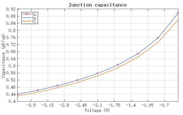
Run the PN_junction_diode_capacitance.msf script, which sets the emitter bias from -0.2 ~ -4 V, automatically runs the simulation, and calculates the variation of the junction capacitance with the bias voltage. In addition, the theoretical capacitance is calculated based on the above simplified expression, as shown in the figure. It can be seen that the simulation results and essentially coincide, and the theoretical value and the simulation curves all decrease with increasing reverse bias, showing the same trend. The theoretical capacitance is slightly lower than the simulation results because the above formula is based on the full depletion approximation, i.e., it assumes that the carriers in the depletion region are completely depleted and that the carrier concentration at the edge of the depletion region changes abruptly. In the actual simulation, however, there is a transition distribution of carrier concentration at the edge of the depletion region, and the contribution of the p-type side to the space charge layer is not strictly zero.