Introduction to Inverse Design
Inverse Design #
This section introduces the basic principles, workflow, optimization methods, and typical applications of inverse design in photonic device design.
Inverse design is an automated structural solving method based on optimization algorithms that can search for photonic device structures meeting target performance within a high-dimensional design space. As integrated photonic devices demand increasingly higher complexity, size, and performance metrics, traditional design approaches relying on manual experience can no longer meet these requirements. Inverse design achieves efficient and high-precision automatic device design through a closed-loop iteration of mathematical optimization combined with physical simulation.
Basic Principles of Inverse Design #
The goal of inverse design is to reduce the designer's workload and improve design efficiency and accuracy through an automated design process. First, a figure of merit (FOM) is defined as the optimization target (such as insertion loss, coupling efficiency, and other key performance indicators). Then, the current structure's actual performance is evaluated using simulation solvers (e.g., FDTD), and mathematical optimization algorithms automatically adjust design parameters until the performance requirements are met.
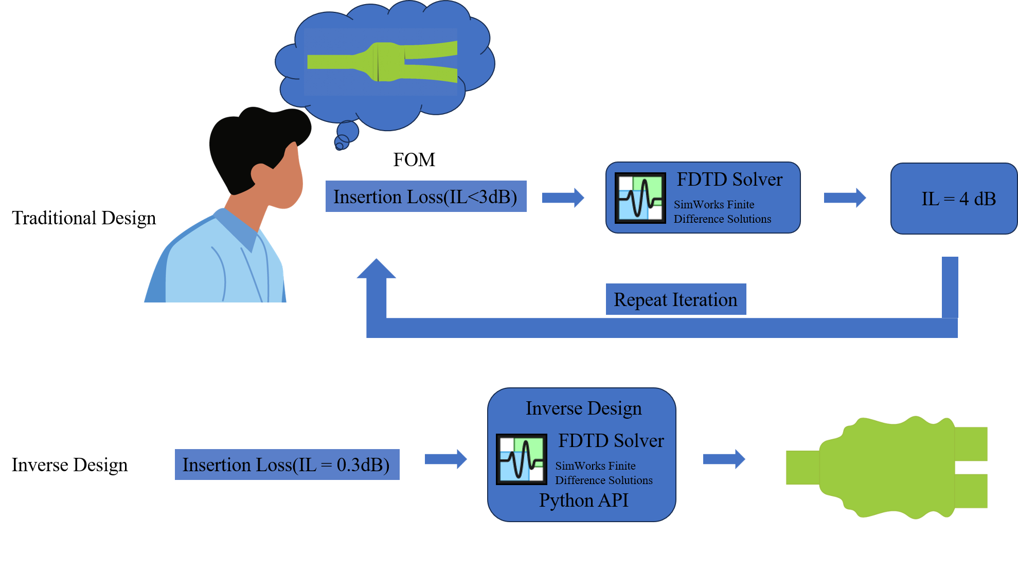
During this process, the optimization algorithm continuously adjusts parameters to explore the entire design space and find the optimal solution. This process is based on physical principles and combined with modern optimization techniques such as gradient optimization and the adjoint method to ensure efficiency and high accuracy.
Gradient Optimization
Gradient optimization is one of the commonly used optimization methods in inverse design. By calculating the gradient of design parameters, the optimization algorithm can quickly converge along the direction of optimal performance. Traditional gradient calculation requires a large amount of computation; for example, if there are 1000 design variables, each variable must be perturbed individually, requiring 1000 repeated simulations to obtain the gradient, resulting in high computational cost. The adjoint method is designed to solve this problem.
Adjoint Method
The adjoint method is a technique for efficiently calculating gradients. The adjoint method simplifies the solution process by transforming the original differential equations into their dual-space form. It requires only two simulations—a forward simulation and an adjoint simulation—to compute the gradient for each parameter. This significantly accelerates the optimization process and greatly reduces computational cost.
Below are some basic principles and applications of the adjoint method:
Taking parameter S as an example, its gradient components can be expressed as:
∇S=(∂p1∂S,...,∂pn∂S)
In the FDTD algorithm, this gradient calculation process can be transformed into a linear algebraic equation, where x represents all electromagnetic field components within the simulation domain.
∂p∂S=∂x∂S∂p∂x
By further differentiating with respect to parameter p and introducing vector V, the gradient expression can be obtained:
∂p∂S=V(∂p∂b−∂p∂Ax)
The meaning of the above expression is: a forward simulation is performed first to obtain all fields x in the simulation domain, which are generated by the source b defined by the specific device. Then, an adjoint simulation is performed, where the adjoint source replaces the forward source b, allowing calculation of V:
ATVT=∂x∂ST
Therefore, the gradient can be calculated after these two simulations.
Workflow of Inverse Design #
The typical workflow of inverse design includes the following steps:
Simulation Setup
Simulation is the core component of inverse design. Users first configure the simulation environment by setting basic parameters such as the operating frequency, material properties, and geometric constraints of the photonic device.
Design Parameterization
Selecting the optimization region and its parameterization method is crucial in inverse design. In the software, users can choose shape optimization and define the design region and parameterization accordingly.
Selection of FOM
Users select an appropriate figure of merit (FOM) based on design requirements. The FOM can be any quantity related to photonic device performance, such as power transmission, bandwidth, or loss. In practice, the FOM is usually calculated through physical simulation.
Optimization Execution
After initializing the optimizer, the algorithm automatically explores the design space, gradually adjusting design parameters to optimize performance. Gradients of parameters are efficiently calculated using gradient optimization or the adjoint method, accelerating the optimization process and eventually converging to the optimal solution.
Result Verification and Adjustment
After optimization, users can verify whether the design meets performance requirements and further adjust design parameters if necessary.
simopt Module
The software currently includes the simopt module, which can directly call related objects to quickly complete inverse design setup. The following introduces the basic setup of a simulation project for the ModeMatch module, which captures power coupling of guided modes.
This module requires the following objects in the project (Its corresponding object name must not be modified.):
- Mode Source (source): Serves as the input source for forward simulation; its size should cover a sufficiently wide span.
- FDFP Monitor for Shape Optimization (opt_fields): Records electromagnetic fields used for shape optimization and serves as the forward simulation result in the adjoint method.
- FDFP Monitor for FOM (fom): Electromagnetic fields recorded by this monitor are used to calculate the target FOM. Multiple FOM monitors can be established in one project. In the adjoint simulation, the adjoint source replaces this monitor.
- Custom Mesh (Mesh): Defines the optimization region, ensuring it is a uniform mesh. The FDFP monitor for shape optimization should be consistent with the mesh region.
- Structure Object: The optimization object structure should be constructed as a polygon type in the simulation.
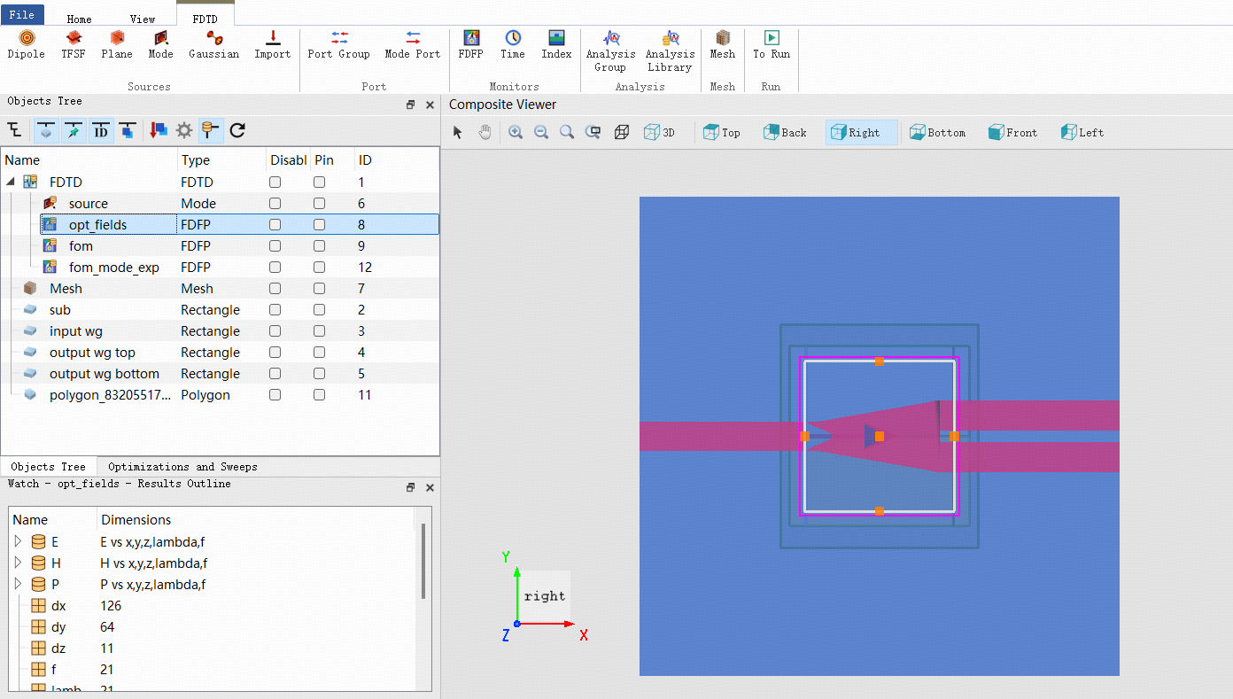
The above is an example project conforming to the ModeMatch module design. The source is the mode source used as the forward simulation input; the opt_fields monitor is the FDFP monitor for shape optimization; the fom and fom_mode_exp monitors can both be used as FDFP monitors to calculate FOM parameters.
The broadband figure of merit expression calculated by ModeMatch is:
FOM=(λ2−λ11∫λ1λ2∣T0(λ)∣pdλ)1/p−(λ2−λ11∫λ1λ2∣T(λ)−T0(λ)∣pdλ)1/p
where T0 is the target transmittance, T is the mode expansion transmittance obtained from actual simulation, λ1 and λ2 are the minimum and maximum wavelengths of the range, and p is the parameter of the generalized p-norm.
Structure Types for Inverse Design #
Inverse design achieves device performance optimization by defining the region and parameters to be optimized. This section introduces two primary optimization methods: Shape Optimization and Topology Optimization.
Shape Optimization
Shape optimization is a design method that fine-tunes the geometric boundaries of a structure with a predetermined topology. Users need to define the initial shape of the device and set key geometric parameters (such as edge coordinates, curvature, etc.) as optimization variables. The optimization algorithm then automatically searches for the optimal combination of these parameters. This method is suitable for performance enhancement of designs that already have a relatively good foundation.
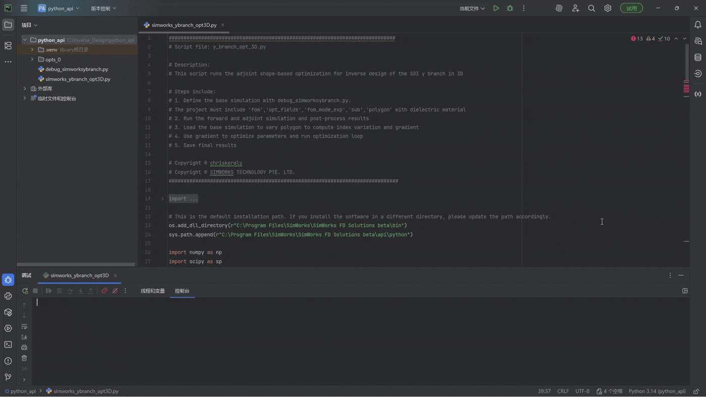
The main workflow is as follows: First, construct the initial device structure using the polygon type in the software. Next, identify geometric features that significantly impact electromagnetic performance and parameterize them as optimization variables. The optimization algorithm automatically adjusts these variables and runs simulations, ultimately finding the combination of geometric parameters that optimizes the Figure of Merit (FOM). To implement this workflow using the Python API, it is necessary to call the FunctionDefinedPolygon series of functions. For more details, see Inverse Design of a Y-branch Splitter.
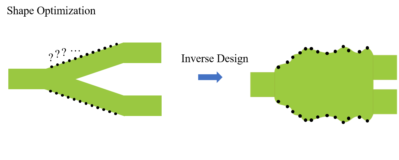
Below is an operational example demonstrating shape optimization:
Topology Optimization
Topology optimization is a more flexible optimization method. Users only need to define the optimizable region and the materials involved. The optimization algorithm can then search for the optimal distribution of material within the entire design space, without relying on any pre-defined geometric shapes. This method can generate highly complex and high-performance designs. However, due to its extremely high degree of freedom, it is usually necessary to introduce manufacturing constraints (such as minimum size limits) during the optimization process to ensure the manufacturability of the final design.
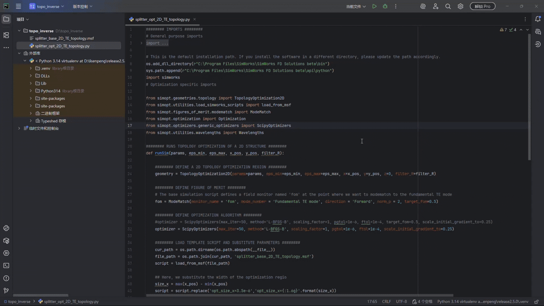
The related 2D topology optimizer is now supported. Its core workflow is as follows: First, discretize each FDTD grid cell within the optimization region into a design parameter representing material density. Initially, based on the starting conditions, these parameters appear as grayscale values that vary continuously between minimum and maximum limits. Next, binarization processing is performed to project these continuous parameters for simulation, where the FOM is evaluated. Subsequently, an adjoint simulation is utilized to obtain the gradient of the FOM with respect to all parameters. The design parameters are then updated based on this gradient, ultimately converging to the optimal design. Throughout this process, constraints must be continuously applied to prevent the feature size of the structure from exceeding practical manufacturing requirements. To implement this workflow using the Python API, it is necessary to call the topology optimization series function TopologyOptimization2D. For details on its usage, please refer to Inverse Design. For a related application example, see 2D Y-branch Based on Topology-Driven Design.

Below is an operational example demonstrating topology optimization:
Application Scenarios #
Inverse design is widely applied in various photonic device fields, including:
- Photonic Integrated Circuits (PICs)
- Micro-optical device design
- Waveguide design
- Beam splitters and filter design
With inverse design technology, engineers can design high-performance photonic devices from scratch, avoiding tedious manual tuning and empirical formulas, thereby improving design efficiency and quality.