Finite Difference Charge Transport(FDCharge) Solver Settings
Finite Difference Charge Transport (FDCharge) Solver #
The Finite Difference Charge Transport Solver (FDCharge) solver is a core simulation tool for modeling the electrical characteristics of semiconductor devices. Based on the classical drift–diffusion model, it accurately computes the internal electrostatic potential distribution as well as electron and hole transport by solving the Poisson equation and carrier continuity equations. This model is well validated and can provide stable and accurate results for a wide range of semiconductor devices under typical operating conditions.
The FDCharge solver is particularly suitable for designing and analyzing the electrical and optoelectronic properties of active photonic devices (for example, MZI modulators and SiGe photodetector).
To create an FDCharge solver, select the FDCharge button in the Home tab and click anywhere in the Composite Viewer window. Then modify the FDCharge solver settings in the automatically opened property editor to complete the addition.
FDCharge Solver Settings #
The FDCharge solver page is shown below. Subsequent sections describe each area in detail.
General Settings #
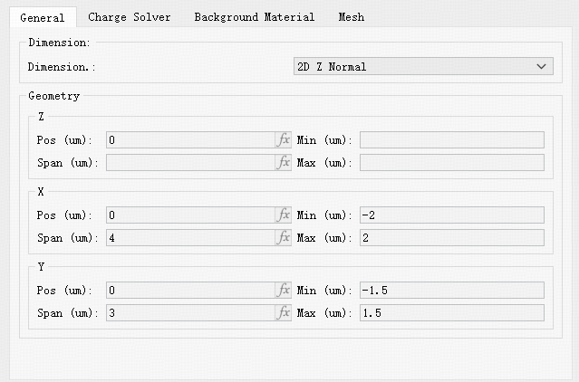
The General tab configures the solver simulation space, including simulation dimension and geometry.
Simulation Dimension #
The Dimension option sets the FDCharge simulation orientation. Currently supported normal directions are: 2D Z normal, 2D X normal, and 2D Y normal.
Geometry #
The Geometry tab sets the FDCharge solver simulation region.
| Name | Description |
|---|---|
| Z / X / Y pos | Set the geometric center of the solver simulation region. |
| Z / X / Y span | Set the extent of the solver simulation region along each coordinate axis. |
Active Solver Settings #
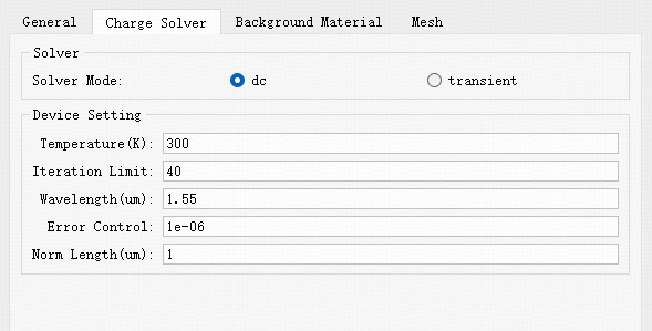
FDCharge provides two active-device algorithms: DC (steady-state) and Transient. Users may choose the appropriate algorithm.
Common settings (DC):
| Name | Units | Description |
|---|---|---|
| Temperature | K | Temperature. |
| Iterations Limit | Total number of iterations. | |
| Lambda | μm | Wavelength. |
| Error Control | Error control settings. | |
| Norm Length | μm | Normalized length — length of the active device. |
Special settings (Transient):
Enabling Transient adds pulse-related options:
| Name | Units | Description |
|---|---|---|
| Timestep | ps | Initial time step for transient simulation. |
| Totaltime | ps | Total simulation time. |
| Shutter Mode | Select pulse mode. on : pulse only during on-time; step on / step off : step-function pulses with on or off times; pulse on / pulse off : pulses with both on and off times. | |
| Shutter on | Set pulse start time. | |
| Shutter off | Set pulse end time. | |
| Shutter tslerw | Step slope. |
![]()
Background Material #
The Background material tab provides a dropdown to select the background material.
| Name | Description |
|---|---|
| Background material | User can directly select materials from the Global Material library within the active exclusive Electrical Material library via a dropdown menu. Alternatively, user can use the Add/Edit function to create project-specific materials in the Project Library for use as background materials. |
Mesh #
The Mesh tab contains solver mesh settings. FDCharge supports uniform meshes and automatic non-uniform meshes. See Mesh Settings for details.
FDCharge Object Settings #
Materials and structures used by the FDCharge solver include active-device specific properties.
Material Settings #
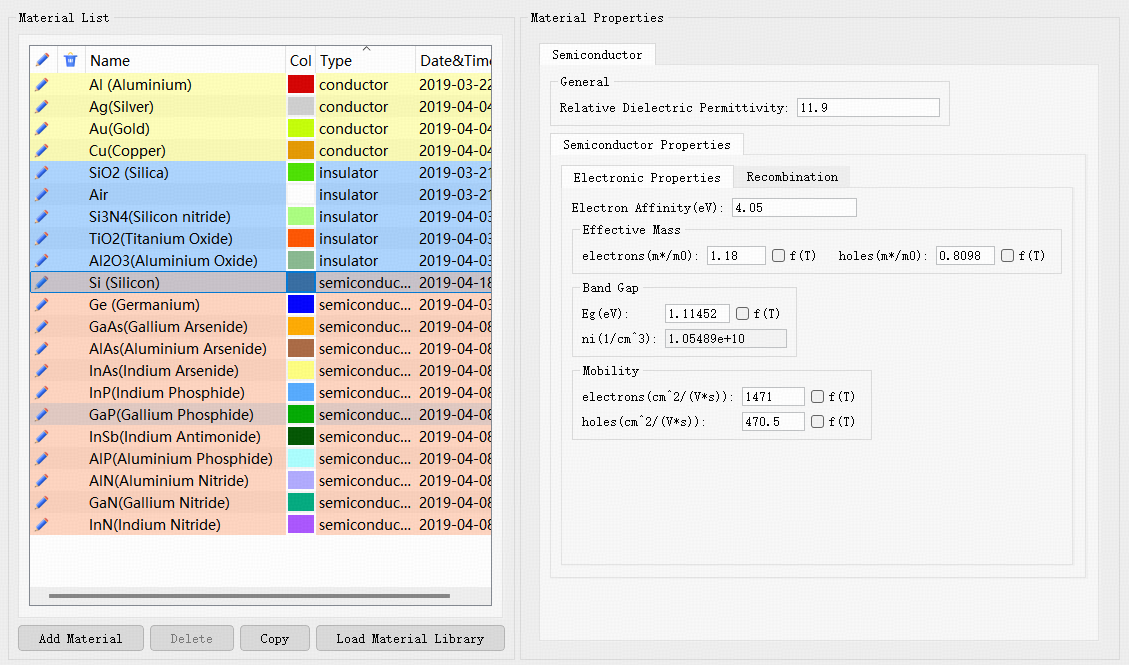
FDCharge uses a dedicated Electrical Material library. The basic material list is similar to passive materials but adds active-device properties under the Semiconductor Properties tab.
Materials are categorized into three classes:
- Semiconductor materials
- Insulator materials
- Conductor materials
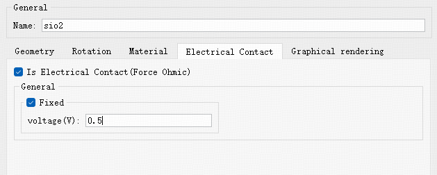
Semiconductor materials are those with Semiconductor Properties defined. Insulators are materials without Semiconductor Properties and materials designated as electrodes. Conductor materials are components marked as electrical contacts in the component list (for example, by enabling Is Electrical Contact and specifying a voltage).
Below are the Semiconductor Properties parameters for semiconductor materials.
| Name | Units | Description |
|---|---|---|
| Electron Affinity | eV | Electron affinity. |
| Effective Mass | Effective mass. electrons: electron effective mass (m*/m0); holes: hole effective mass (m*/m0). | |
| Band Gap | Band gap. Eg: bandgap; ni: intrinsic carrier concentration. | |
| Mobility | Carrier mobility. electrons: electron mobility; holes: hole mobility. | |
| Recombination | Carrier recombination settings. Enable Shockley-Read-Hall: enable SRH recombination model and set electron/hole lifetimes; Enable Radiative: enable radiative recombination; Enable Auger: enable Auger recombination. |
Structure Settings #
Structures in the FDCharge solver have active-device related settings described in the material section. Components with the Is Electrical Contact option checked are treated as electrodes, and the corresponding material is treated as a conductor.