
Application Gallery
OLED
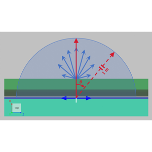
Organic light-emitting diode (OLED) devices are widely used in high-end displays and solid-state lighting due to their self-emissive nature, wide viewing angle, high contrast ratio, and compatibility with flexible form factors. A typical OLED consists of multiple organic functional layers and electrodes, with a total thickness usually on the sub-micrometer scale. In such a multilayer optical environment, radiation generated by dipole emitters in the emissive layer is strongly influenced by optical confinement and interference effects. In addition, refractive index discontinuities between functional layers cause a large portion of the emitted light to be trapped inside the device in the form of waveguide modes or surface plasmon polariton modes, so that only a small fraction can escape into air. As a result, accurate modeling of multilayer optical behavior, combined with micro- and nanostructure design to enhance light extraction efficiency (LEE), is a key challenge in OLED optical design. In this case, a 2D FDTD method is used to model an OLED device. By comparing structures without microstructures and with periodic microstructures (photonic crystals), the effect of microstructure design on LEE is evaluated.