
Application Gallery

Fresnel Lens
By employing a distinctive “concentric stepped ring” structure, the Fresnel lens decomposes the continuous surface of a conventional lens into multiple “annular micro-lenses,” each functioning as an independent refracting surface. This design dramatically reduces the lens thickness and mass while maintaining focusing or imaging performance comparable to that of a traditional convex lens. Because of this thin and lightweight architecture, Fresnel lenses are widely used in lighthouse illumination, projection systems, solar concentrators, and compact imaging devices—particularly in applications where high focusing efficiency is required under tight volume and cost constraints. In this case, a 2D FDTD simulation is performed for a Fresnel lens derived from a spherical lens profile, demonstrating its wavefront-shaping capability and characteristic phase behavior.
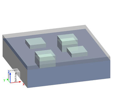
Lithography Using Alternating Phase Shift Mask
The demand for smaller, faster, and lower power semiconductor devices continuously drives advances in optical lithography technology. As the size of semiconductor devices continues to shrink, it is necessary to use alternating phase shift masks (APSM) to improve resolution. For example, at the 45nm node, some features to be imaged are smaller than the diffraction limit of the 193nm light source used. APSM modulates the phase so that the light interferes with itself after passing through the mask, making the mask pattern edges sharper and clearer, thereby improving pattern contrast. The proximity effects occurring at sub-wavelength scales need to be understood through lithography simulation, so they can be accounted for in mask design, ensuring a predictable and reliable process. This case demonstrates how to image sub-wavelength features using APSM in FDTD.
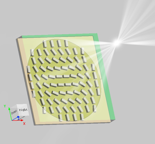
Metalens Based on PB Phase
Traditional curved optical lenses rely on phase accumulation along the light path to control light, which is limited by the refractive index of natural materials. To correct various image aberrations, multiple lenses are usually needed. However, combining multiple optical lenses occupies a lot of space, making it difficult to miniaturize optical systems. Metalenses, however, manipulate incident light to bend beams through the arrangement of artificial sub-wavelength units on the dielectric surface. A single metalens can achieve the same performance as a device that requires multiple optical lenses. Compared to traditional optical lenses, metalenses are smaller, lighter, cheaper, have better imaging quality, and are easier to integrate. They provide a new solution for compact integrated optical systems. This case study, based on the research of Xicheng Xia and Zan Yao, introduces how to use FDTD to simulate metalenses, helping readers achieve miniaturization of optical systems.