2D三角晶格能带结构
前言
在 2D 光子晶体中,不同的晶格类型拥有完全不同的能带结构。对不同晶格类型的模型使用 FDTD 求解器进行仿真时,基础设置也不相同。本案例构建了平行排列的空气圆柱形成的 2D 三角晶格光子晶体的模型,并计算了其能带结构,据此介绍了在对非矩形晶格光子晶体进行 FDTD 仿真时的一些特殊设置及注意事项。
仿真设置
模型简介
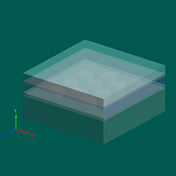
本案例使用 FDTD 分析由均匀介质中周期性排列的空气圆柱组成的三角晶格光子晶体的能带结构。与 2D 方晶格光子晶体类似,均匀介质中的空气圆柱周期性排布同样实现了空间中周期性变化的折射率分布,形成了光子带隙,阻碍部分特定频段的光进入结构内部。本光子晶体模型中,介质材料的折射率为 2,周期性排布的空气圆柱的半径 为 200 nm,构成的三角晶格的晶格间距 为 500 nm。对于这种非矩形晶格结构的光子晶体,在 FDTD 仿真区域中至少包含两个晶格单元。
模型构建
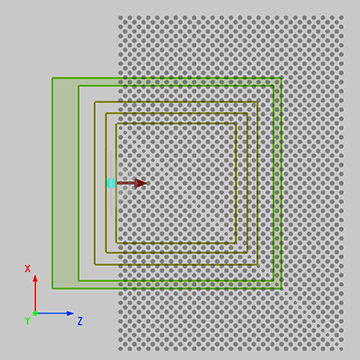
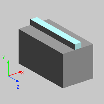
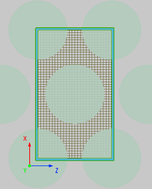
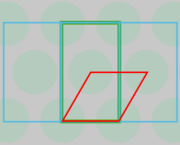
本案例的仿真设置与案例2D 正方晶格能带结构相似,在此不再重复,请下载工程文件附件 triangular_2D.mpps 查看详细信息。由于 FDTD 仿真区域的形状被矩形网格所限制,所以非矩形晶格结构无法像矩形晶格结构一样仅选择一个完整的晶格周期单元进行仿真。对于 2D 三角晶格或其他非矩形晶格的光子晶体,只能对整体晶格结构进行矩形区域划分,选择适合 FDTD 求解器的矩形周期性结构模型。如下图所示,三角晶格结构可以看作是被一个个绿色线框内的矩形结构按方形晶格排布而成的。所以将仿真区域选择为和线框一致,对其中的结构模型进行仿真。
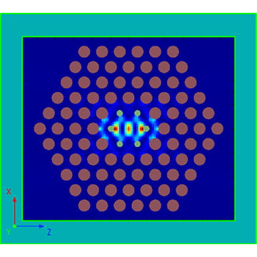
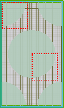
需要注意的是,要保证每个光子晶体结构单元的网格剖分方式及尺寸相同。确保折射率分布的统一性和周期性,以免造成计算结果不准确的现象。如下图所示,虚线框内对比了不同结构单元对应位置的网格分布。明显看出每个圆形结构区域的网格剖分方式相同。这就要求仿真区域内的网格数必须为偶数,并且网格关于仿真区域中心坐标轴呈对称分布(在求解器高级设置页面,勾选 Mesh Generation 中的 force symmetric x/z mesh 选项,强制构建关于 X/Z 轴对称的网格)。
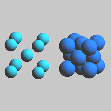
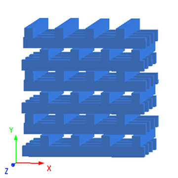
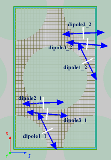
对于仿真区域中包含多个晶胞的模型,为了避免人工区域折叠的问题,我们必须在每个晶胞中均设有相匹配的偶极子源,并且每一组匹配的偶极子源在晶胞内的位置要完全相同。偶极子源之间的相位差 必须满足公式 : ,其中 为仿真的波矢, 为两偶极子源的位置变化矢量。分析组 Dipole Clouds 的内置脚本会完成这种偶极子源阵列的构建,仅需根据光子晶体模型设置好分析组内的变量参数值。如图所示,三组相匹配的偶极子源被构建完成。
仿真结果
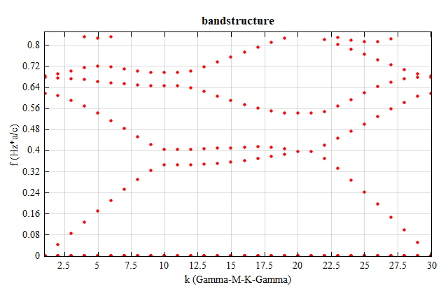
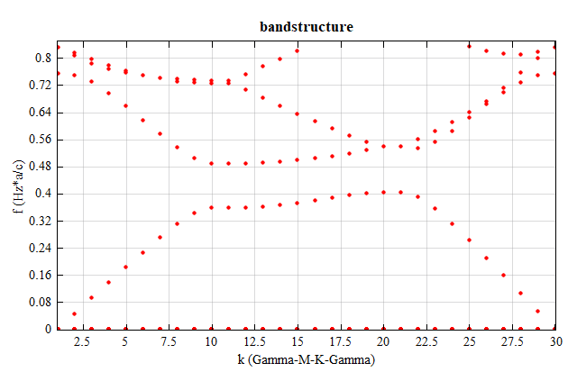
下载并打开附件中的工程文件 triangular_2D.mpps,运行所有的参数扫描后,运行脚本文件(triangular_2D.msf)获取扫描结果,并绘制 TE 模式下能带结构图,如下图所示。
可以通过改变求解器属性中的偏振类型计算得到 TM 模式下的能带结构,如下图所示。