基于拓扑逆向设计的二维Y分束器
前言
近年来,逆向设计(inverse design)已经成为光子器件开发中的重要方法论。相比传统依赖经验、直觉或大量参数扫描的正向设计流程,逆向设计将器件开发重新表述为一个具有明确性能指标的优化问题。通过设定期望的电磁响应,并允许算法在设计空间中自由搜索,逆向设计能够自动生成许多难以通过人工经验推导的高性能光子结构。
在Y分束器的逆向设计案例中,我们展示了二维Y分束器的参数化逆向设计方法,通过自动优化少量几何控制参数,实现了器件性能的显著提升。然而,参数化设计本身仍然需要预先假设结构形式,其设计自由度在一定程度上受到限制。
在本案例中,我们进一步针对二维Y分束器引入拓扑逆向设计(Topology Optimization)方法,不再对器件几何形态作任何先验假设,而是直接在设计区域内对材料分布进行优化,从而显著拓展了设计自由度,本案例展示了拓扑逆向设计在光子器件结构生成与性能优化中的强大能力。
仿真设置
本案例中的完整仿真与优化流程由附件中的 Python 脚本 splitter_topology_2D_TE.py 自动驱动。整个流程完全基于 SimWorks 提供的 Python 接口与逆向设计优化框架实现,无需人工在软件界面中手动搭建结构或配置光源。有关该优化框架的完整理论说明与接口使用方法,可参考用户手册中的逆设计介绍。
脚本的整体结构与Y分束器的逆向设计案例基本一致,主要包含以下几个核心模块。
-
基础环境配置
脚本首先完成软件接口路径的配置,并导入必要的 Python 依赖库,包括数值计算库NumPy以及 SimWorks 的Python API。import os import sys # This is the default installation path. If you install the software in a different directory, please update the path accordingly. os.add_dll_directory(r"C:\Program Files\SimWorks\SimWorks FD Solutions\bin") sys.path.append(r"C:\Program Files\SimWorks\SimWorks FD Solutions\api\python") import numpy as np import simworks随后,脚本加载 SimWorks 拓扑优化相关模块,包括拓扑几何描述、目标函数定义以及优化器接口。这些模块共同构成了一个完整的自动化逆向设计框架。
-
拓扑几何建模
与Y分束器的逆向设计案例中采用的“控制点 + 样条插值”的参数化几何方法不同,本案例采用基于像素化设计区域的拓扑优化策略。
在器件的分束区域内定义一个二维拓扑优化区域,并将其离散为规则的网格像素。每一个像素对应一个连续设计变量,用于描述该位置处的等效介电常数,其取值范围被限制在包层材料与波导材料之间。
拓扑优化区域通过
TopologyOptimization2D类进行定义,其核心参数用于描述设计变量的初始状态、材料约束以及空间离散方式,具体如下所示:geometry = TopologyOptimization2D( params=params, eps_min=eps_min, eps_max=eps_max, x=x_pos, y=y_pos, z=0, filter_R=filter_R )其中各参数的物理含义如下:
-
Params
用于定义拓扑优化的初始设计变量分布,既可以作为初始几何条件,也可以在多轮优化过程中传入上一轮迭代结果,用于继续优化。 -
eps_min
设计区域内允许的最小介电常数,对应包层材料的介电常数,用于限定低折射率区域的物理下限。 -
eps_max
设计区域内允许的最大介电常数,对应波导核心材料的介电常数,用于限定高折射率区域的物理上限。 -
x、y
分别表示拓扑优化区域在 x 和 y 方向上的空间坐标,用于定义设计变量与 FDTD 网格单元之间的空间映射关系,从而实现二维拓扑建模。 -
z
拓扑优化区域在 z 方向上的位置。由于本案例为二维拓扑结构设计,该参数固定为0。 -
filter_R
Heaviside 滤波器的半径参数,用于对设计变量进行空间平滑处理,以抑制过小特征尺寸并提高结构的可制造性与数值稳定性。
在本案例中:像素尺寸为 ;优化区域长度约为 ;利用结构对称性,仅对上半区域进行优化。这种拓扑建模方式极大地提升了设计自由度,使算法能够在无需预设几何形态的情况下,自主生成高性能结构。
-
-
材料参数与初始条件
拓扑优化区域内的材料参数设置如下:
最小介电常数:
最大介电常数:
其中, 并非硅的本征介电常数,而是由三维硅波导在给定厚度条件下的基模有效折射率计算得到,用于表征硅波导在二维仿真中的等效电磁响应。因此,尽管拓扑优化过程在二维平面内进行,该建模方式本质上反映的是一种 准三维仿真近似。
为避免对最终结果施加人为几何偏置,初始条件设置为整个设计区域内介电常数的均匀中间值:
initial_cond = 0.5 * np.ones((x_points, y_points))该设置使优化过程完全由性能目标驱动,而非初始结构假设。
-
优化问题构建
目标函数定义
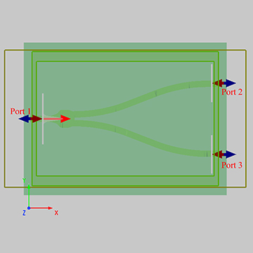
与前一案例类似,本案例的优化目标通过 Mode Match 模块定义。在输出端口处设置场监视器,对传播方向上的基模 TE 模式进行模场匹配评估。
fom = ModeMatch(
    monitor_name='fom',
    mode_number='Fundamental TE mode',
    direction='Forward',
    norm_p=2,
    target_fom=0.5
)
目标函数反映了输出端口处目标模式的激励效率,对应于期望的等功率分束行为。
多波长优化设置
为提升器件在实际应用中的带宽性能,优化过程在 至 波段内同时进行,共选取 11 个离散波长点:
wavelengths = Wavelengths(start=1450e-9, stop=1650e-9, points=11)最终的优化目标为多波长条件下的综合性能。
优化算法与平滑约束
优化器选用
L-BFGS-B拟牛顿算法,其在高维连续变量优化问题中具有良好的收敛效率。optimizer = ScipyOptimizers( max_iter=50, method='L-BFGS-B', pgtol=1e-6, ftol=1e-4, scale_initial_gradient_to=0.25 )为确保最终结构的可制造性,并抑制非物理的小尺度特征,在每次迭代中对设计变量施加空间平滑滤波。滤波半径对应于约 的物理尺度,用于消除尖角和细小孤立结构。
-
自动化优化流程
在整合上述模块后,脚本启动一个完全自动化的拓扑逆向设计闭环,其流程如下:
-
根据当前设计变量更新设计区域内的介电常数分布;
-
自动调用 SimWorks 执行电磁仿真;
-
计算输出端模场匹配度作为目标函数值;
-
基于伴随法计算目标函数对所有像素变量的梯度;
-
由优化器更新设计变量。
该过程持续进行,直至目标函数收敛或达到最大迭代次数。
-
仿真结果
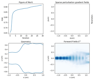
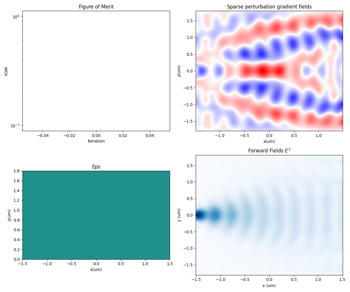
为展示拓扑逆向设计过程中结构形态与器件性能的演化趋势,首先给出优化初始阶段的仿真结果。下图展示了初始条件下设计区域内的介电常数分布及对应的光场传播情况。可以看到,此时分束区域为均匀介质填充,缺乏有效的能量引导结构,光场在分束区域内产生明显散射与辐射损耗,整体分束效率较低。
随着优化迭代的推进,算法逐步在设计区域内“雕刻”出具有明确功能性的介质分布形态。原本连续均匀的材料分布逐渐演化为清晰的能量传输通道,使输入光场能够更高效地完成分束过程。
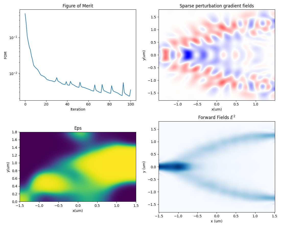
在拓扑逆向设计过程中,程序会在每一次迭代结束后自动保存当前设计状态。具体而言,每一代迭代都会生成一个对应的 .npz 数据文件,用于记录该次迭代下的拓扑设计变量分布以及对应的目标函数评估结果。
借助这些中间结果文件,可以完整重构优化过程中设计区域内介电常数分布的演化轨迹,并对目标函数的收敛行为进行后处理分析。这一机制使拓扑优化流程具备良好的可追溯性与可复现性,用户不仅可以对优化路径进行可视化,还可以对中间结构进行筛选或进一步加工处理。
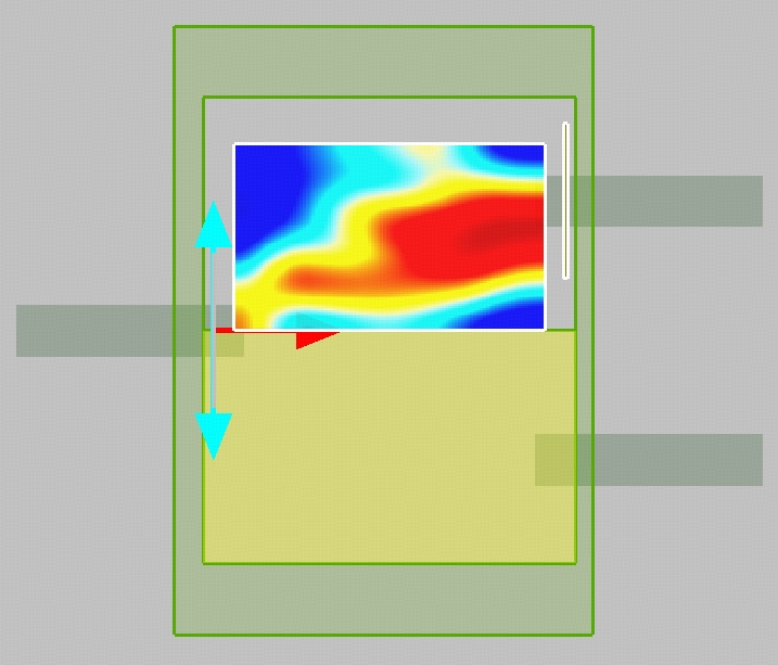
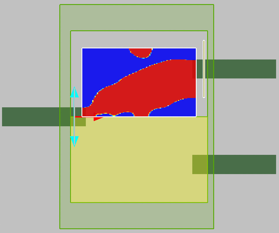
最终得到的拓扑优化结构如下图所示,可直接在 SimWorks 软件中打开,并进行更精细的电磁性能分析。
对应的最终光场传播分布如下图所示,可以观察到输入光能量被平滑且对称地引导至两个输出端口,分束区域内的辐射损耗显著降低。
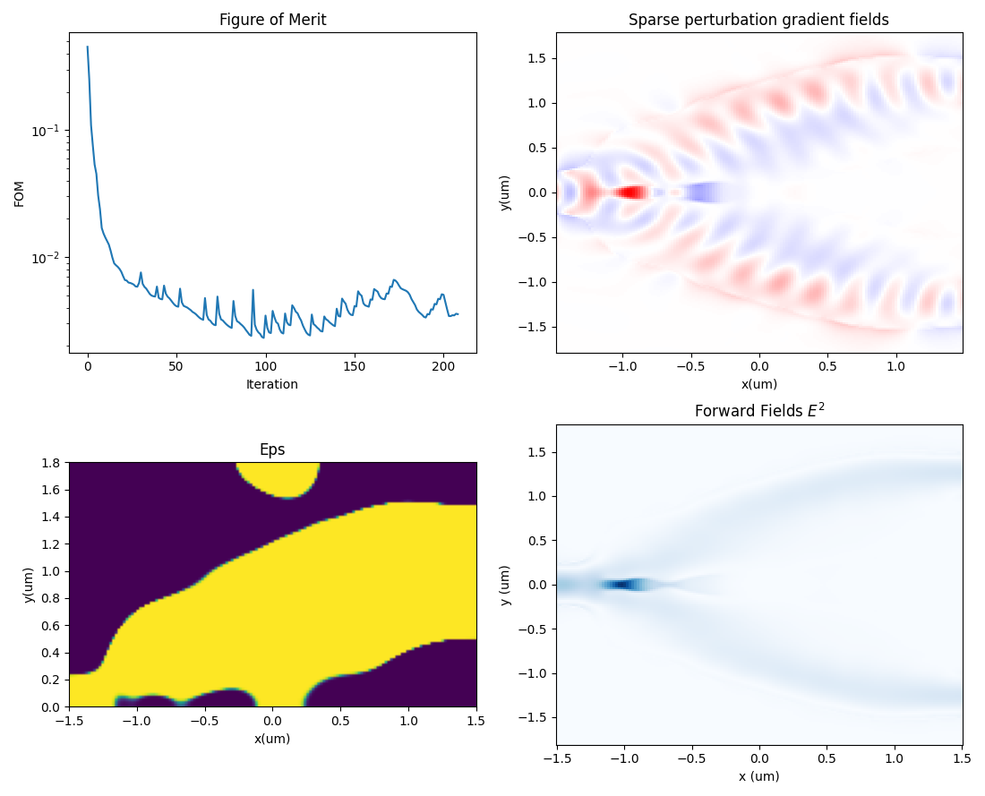
结果表明,经过拓扑逆向设计优化后,该 Y 分束器在目标波长范围内实现了稳定的等功率分束行为,并在有限尺寸条件下展现出良好的带宽性能。这一结果进一步验证了拓扑逆向设计方法在复杂光子器件自动生成中的有效性与工程实用价值。
相关视频