Contact Number
Email
 Enterprise WeChat
 WeChat Service Account
 Wechat Channels
This section introduces the FDCT simulation control panel.
The Finite Difference Carrier Transport (FDCT) solver resolves Poisson and carrier transport equations for active photonic devices and is suitable for simulating carrier transport in semiconductor devices.
The control panel contains buttons and displays for basic active-device settings and simulation information, as shown below:

| Name | Description |
|---|---|
| Design | To Design: return to simulation design. |
| Simulation Info | Simulation information. |
| Simulation Setting | Simulation settings. |
| Progress | Shows simulation progress. |
| Status | Shows simulation status. |
| Run DC Simulation | Run active (DC) simulation. |
| Tool | Controls opening and clearing of data files. |
This area displays the project's simulation information.
| Name | Description |
|---|---|
| Dimension | Simulation dimensionality. |
| Is Doped | Whether the project includes doping. |
| Generation | Whether photogeneration (generation rate) is imported. |
These settings match the FDCT solver settings.
| Name | Units | Description |
|---|---|---|
| Temperature | K | Temperature. |
| Iterations Limit | Total number of iterations. | |
| Lambda | Wavelength. | |
| Error Control | Error control. | |
| Norm Length | Normalized length; length of the active device. |
The FDCT solver includes features different from passive solvers, such as independent doping settings and active-parameter monitors. The feature buttons are shown below:
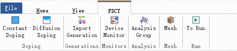
| Name | Description |
|---|---|
| Constant Doping | Add uniform doping; defines a region with uniform dopant concentration. |
| Diffusion Doping | Add diffusion doping; define a region with dopant distribution function. |
| Import Generation | Import generation rates produced by passive simulations (commonly used for photodetector designs). |
| Device Monitor | Add device (active) parameter monitors to record optical/electrical fields in a region. |
| Analysis Group | Add analysis groups. |
| Mesh | Add custom mesh. |
| To Run | Run simulation. |
These FDCT settings define doped semiconductors. Note: Doping applies only to semiconductor materials; doping in non-semiconductor regions is automatically ignored during computation, so you do not need to worry if a doping region overlaps non-semiconductor regions.
Two doping methods are supported: uniform (constant) doping and functional (diffusion) doping. Doping contributions are cumulative: if multiple doping objects apply to a region, the net doping is the sum of their concentrations. N-type and P-type dopants have opposite signs and will partially cancel each other.
Defines a semiconductor region with a fixed dopant concentration. Users specify the geometry and parameters of the region.
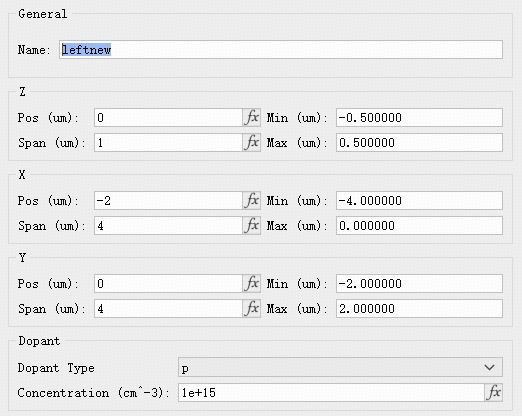
Parameters:
| Name | Description |
|---|---|
| General | Set the doping object's name. |
| X / Y / Z | Set the center position and extent of the doping region. |
| Dopant | Doping settings. Dopant Type: choose p for hole (acceptor) or n for electron (donor). Concentration: dopant concentration in atoms per cubic centimeter (). |
Functional doping defines concentration by a distribution function. Two distribution types are supported: 1) constant surface-source diffusion (erfc function) and 2) finite surface-source diffusion (gaussian function).
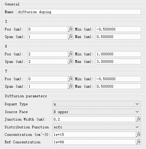
Parameters:
| Name | Description |
|---|---|
| Dopant Type | Choose dopant type: p for holes (acceptors), n for electrons (donors). |
| Source Face | The face where doping is injected. |
| Junction Width | Width over which concentration drops from maximum to minimum according to the distribution. |
| Distribution Function | Select the doping distribution function. |
| Concentration | Maximum dopant concentration (atoms per ). |
| Ref Concentration | Minimum dopant concentration (atoms per ). |
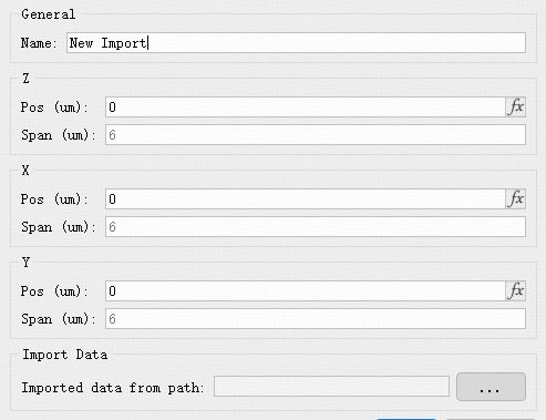
This option imports photogeneration (generation rate) results produced by a passive simulation. It is commonly used in photodetector simulation designs.
The FDCT solver provides Device monitors (active parameter monitors). Monitors are typically set to match the FDCT simulation region.
Device monitors can record optical, electrical, and other related quantities. The available parameters are:
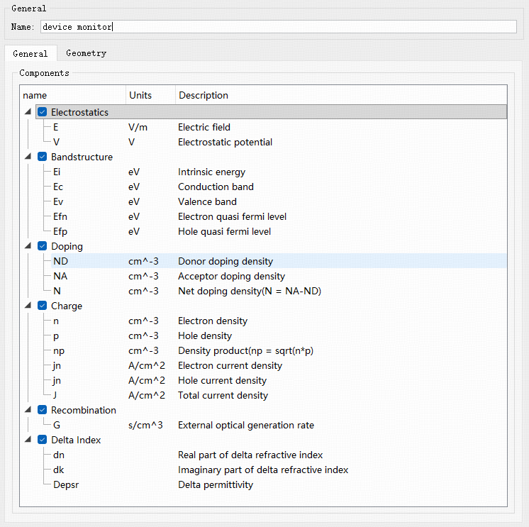
| Name | Physical Quantity | Units | Description |
|---|---|---|---|
| Electrostatics | E | V/m | Electric field. |
| V | V | Electric Potential | |
| Ei | eV | Intrinsic energy. | |
| Ec | eV | Conduction band. | |
| Bandstructure | Ev | eV | Valence band. |
| Efn | eV | Electron quasi-Fermi level. | |
| Efp | eV | Hole quasi-Fermi level. | |
| ND | Donor concentration. | ||
| Doping | NA | Acceptor concentration. | |
| N | Net doping density (N = NA - ND). | ||
| n | Electron concentration. | ||
| p | Hole concentration. | ||
| Charge | np | Charge product (np = sqrt(n * p)). | |
| jn | Electron current density. | ||
| jp | Hole current density. | ||
| J | Total current density (jn - jp). | ||
| Recombination | G | Imported generation rate. | |
| dn | Change in n. | ||
| Delta Index | dk | Change in k. | |
| Depsr | Change in permittivity. |
