使用单个亚波长孔径聚焦
前言
亚波长光学器件在光场调控和光子集成领域具有广阔的应用前景。相比传统光学器件,它们能够在远小于工作波长的尺度上操控光场,实现更高的集成度与功能密度。特别是聚焦型亚波长光学器件,能够有效提升光的方向性与能量集中度,在微纳尺度下实现远场聚焦,为高分辨率成像、近场探测以及光通信中的高效耦合提供了新的可能。
然而,在亚波长尺度下,光会发生强烈的干涉和衍射,使得聚焦变得困难。Garcia-Vidal[1] 等人提出了一种结构:在金属薄膜中开设单一亚波长孔径,并在孔周围引入表面沟槽,通过激发表面等离激元实现远场聚焦。本案例对该结构进行了建模仿真,并对焦斑宽度进行了分析,以展示其聚焦性能。
仿真设置
模型简介
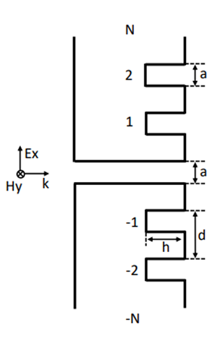
本案例采用的模型如上图所示,结构在输出表面设计有 20 个周期为 的凹槽,凹槽深度为 ,其宽度与中央亚波长孔径的宽度均为 。由于 Garcia-Vidal[1:1] 的理论计算中假设金属为理想导体,因此仿真中采用完美电导体(PEC)材料建模。
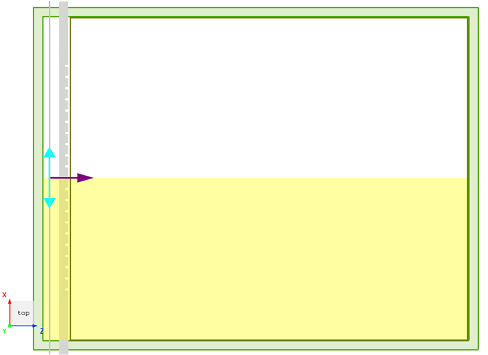
光源为波长范围 的平面波,从结构左侧入射。考虑到结构和光源的对称性,在 方向采用 Anti-Symmetric 反对称边界条件,将仿真区域缩小至一半以提高效率,其余边界均设置为 PML。在平面波两侧使用 PML 会引入衍射和边缘效应,导致光源无法在全区域保持理想的平面传播。但在本案例中,亚波长孔径位于仿真的中心区域,且仿真宽度远大于亚波长孔径,因此孔径处几乎不受边缘效应影响;同时,靠近 PML 边缘的场畸变会被 PEC 金属板反射,因而不会进入中心孔径,对结果分析的影响可以忽略。
仿真结果
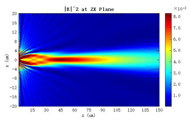
仿真完成后,运行附件中的 Focusing_with_slit.msf 脚本,可以得到亚波长孔径输出后的电场分布结果。
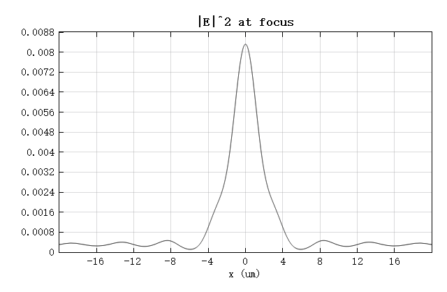
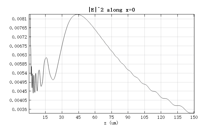
在 处提取的电场强度分布如图所示。结果显示,透过亚波长孔径的光场在远场被有效聚焦,焦点位置约在 ,对应的电场强度约为 。
平面上的电场强度分布如图所示,可以直观地看到光场从孔径出射后逐渐汇聚并在焦点附近形成高强度区域。为更清晰展示聚焦效果,需将 colorbar max 设置为焦点处电场强度。
在焦点位置沿 方向的电场强度分布如图所示。其全宽半高(FWHM)约为 ,验证了该结构在远场实现了亚波长聚焦效果,结果与 Garcia-Vidal[1:2] 的研究结论基本一致。